




In high-volume SMT lines, a board that clears automated optical inspection can still leave the factory with undetected opens, solder bridges under QFNs, or polarity-reversed diodes. Functional testing later in the process often reveals these only after the product has already consumed test time and handling resources. Bed-of-nails in-circuit testing remains the most practical method for catching parametric defects early, yet many layouts still reach the fixture with coverage below 70 percent. The result is either expensive flying-probe fallbacks or, worse, field returns. Production experience shows that the difference between a reliable ICT station and a daily bottleneck almost always traces back to design-for-test decisions made months earlier.

Why Test Access Still Fails on Modern Assemblies
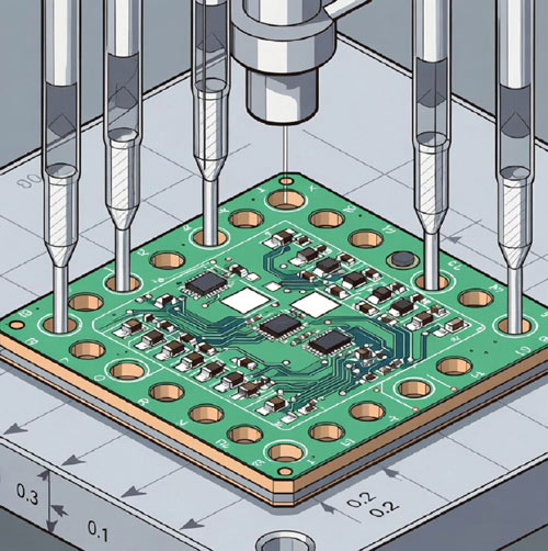
Dense component placement, buried vias, and bottom-side connectors leave large portions of the netlist unreachable. When test pads are omitted or placed under tall parts, the fixture simply cannot contact the node. Factories routinely see first-pass ICT yields drop 15–25 percent on such boards compared with DFT-compliant designs. Alignment becomes another silent killer: tooling holes held only to ±0.1 mm allow the board to shift under pneumatic pressure, producing intermittent contacts that operators misdiagnose as component failures. Warpage after reflow further compounds the problem on thin cores; pins land on the edge of pads or miss entirely. These mechanical realities turn what should be a 10-second parametric screen into a source of false failures and rework.
Pin Force, Warpage and Guarding: What the Fixture Really Demands
Spring-loaded pins deliver reliable contact only within a narrow force window—typically 50–150 g per pin. Too little force yields high-resistance readings; too much risks pad cratering or board flex. Stroke length of 1–2 mm accommodates modest warpage, but only if the fixture distributes pressure evenly. Guarding circuits are equally critical: without them, parallel paths through adjacent components corrupt resistance and capacitance measurements. Fixture wiring must stay short and shielded; otherwise noise floors rise and measurement repeatability collapses after a few thousand cycles.
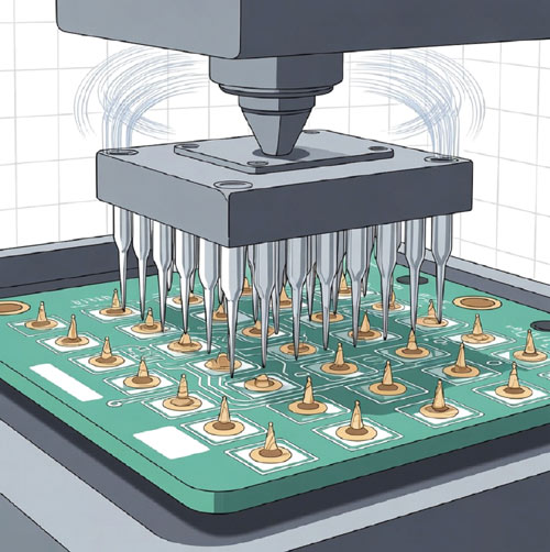
Custom fixtures amortize only when volumes exceed several hundred units. Below that threshold the mechanical design, pin mapping, and program debug often outweigh the test-time savings. This economic boundary, more than any technical limitation, explains why many teams still default to flying probes for prototypes and early production.
Layout Practices That Consistently Deliver High Coverage
Successful bed of nails PCB implementations begin with consistent pad sizing and grid alignment. Test pads of 0.8–1.0 mm diameter with 0.5 mm edge clearance from solder mask and silkscreen give the pins a forgiving target while avoiding solder-mask shorts. Placing every accessible pad on a 100-mil grid allows the fixture builder to use standard pin arrays, cutting both cost and lead time. Tooling holes of 3.2 mm diameter held to ±0.05 mm, located near opposite corners, eliminate the registration drift that produces intermittent failures. Preferring a single side for probing simplifies the fixture and reduces pin count; when double-sided access is unavoidable, staggered tooling pins maintain alignment under pressure.
Via-in-pad or short breakout stubs on BGA power and ground nets recover 15–20 percent additional coverage that would otherwise remain hidden. Early extraction of the netlist into fixture-design software reveals unreachable nodes while the layout can still be corrected. Prototype runs on a golden board then establish realistic measurement limits that account for tolerance stack-up rather than ideal component values.
| Design Decision | Fixture Cost Impact | Coverage Impact | Yield / Repeatability Effect |
|---|---|---|---|
| 100-mil grid test pads | Lower (standard pins) | High | Stable contacts, fewer false fails |
| Scattered or missing pads | Higher (custom dense array) | Low (<70%) | Intermittents, more rework |
| Tooling holes ±0.05 mm | Neutral | High | Reliable registration |
| Tooling holes ±0.1 mm | Neutral | Reduced | Daily misalignment stops |
| Via-in-pad for BGA nets | Modest increase | +15–20% | Fewer power-domain escapes |
Mistakes That Still Appear in DFM Reviews
Layouts continue to arrive with test pads centered under connectors or shielded modules, guaranteeing zero access. Designers often size pads to the minimum land of a discrete component and then forget the 0.5 mm clearance requirement, resulting in solder-mask bridges once the pins apply force. Another recurring error is treating ICT as an afterthought: the board is optimized solely for flying-probe access, then forced onto a bed-of-nails fixture late in the program. Component tolerance windows are set to catalog limits without manufacturing margin, so normal process variation generates false failures. Finally, boards thinner than 1.0 mm receive no additional support points; the resulting flex produces open readings that disappear once the board is removed from the fixture.
A Practical Checklist Before Releasing Gerbers
● Assign a test pad to every net that can be reached without violating keep-out zones; prioritize power, ground, and high-value passives.
● Enforce 0.8–1.0 mm pad diameter and 0.5 mm clearance on a 100-mil grid.
● Specify tooling holes to ±0.05 mm and locate them for balanced clamping.
● Confirm single-sided probing is feasible; if not, plan staggered double-sided access early.
● Extract the netlist and run a virtual probe placement before final artwork.
● Build measurement limits from actual golden-board data rather than ideal values.
● Schedule a fixture debug run on the first article so program and mechanical issues surface before volume starts.
Key Takeaways for Production Engineers
Bed-of-nails ICT delivers its highest value only when the board is designed for it from the schematic stage. The mechanical constraints of pin force, alignment, and warpage are not optional details—they determine whether the station runs at full throughput or becomes a daily source of false calls. Layouts that respect simple rules of pad size, grid, and tooling tolerance consistently achieve coverage above 90 percent and first-pass yields that repay the fixture investment within a few hundred boards. Those that ignore them force production into slower, more expensive alternatives and leave residual risk that only appears after the product ships. In high-volume environments the difference is measured not in theory but in scrap, downtime, and field returns.

