Can packaging unlock the next leap in AI chips? Advanced interconnect technologies are pushing semiconductor integration beyond reticle limits.
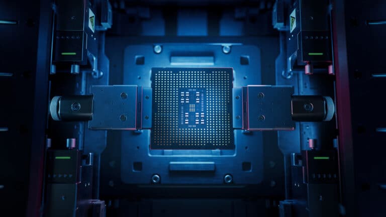
Intel Foundry has highlighted its advanced semiconductor packaging technologies that combine multiple chiplets into a single high-performance package, enabling artificial intelligence (AI) processors to overcome the size and performance constraints of monolithic chips. The company says its packaging portfolio, centred on Foveros, EMIB and EMIB-T, is helping scale complex AI processors while improving power delivery and interconnect efficiency.
As AI workloads continue to grow, semiconductor manufacturers are increasingly adopting chiplet-based architectures instead of producing larger single dies. Advanced packaging enables different functional chiplets, including compute, memory and I/O, to operate as a unified system, allowing designers to bypass reticle-size limitations while improving manufacturing flexibility and yield. According to Intel, its New Mexico facility can currently support package sizes up to eight times the industry-standard reticle limit, with plans to exceed twelve times that scale by 2028.
Foveros provides three-dimensional integration by stacking specialised chiplets on a silicon base, allowing components fabricated on different process nodes to function together within a compact footprint. The company says the approach supports higher performance while improving power efficiency in applications ranging from edge devices to AI accelerators.
Complementing this, embedded multi-die interconnect bridge (EMIB) technology links adjacent chiplets using embedded silicon bridges instead of full silicon interposers, reducing manufacturing complexity and enabling high-bandwidth communication between dies. The latest EMIB-T extends this architecture by incorporating power delivery channels directly through the bridge, improving signal routing and supporting the bandwidth demands of high-bandwidth memory (HBM)-based AI processors.

The technologies are being deployed at Intel’s advanced packaging facility in Rio Rancho, New Mexico, where the company is expanding domestic packaging capabilities for next-generation semiconductor products.
“Some of the customers are coming to us first for advanced packaging. When we’re successful delivering to those customers, they’ll continue to grow their trust and faith in Intel as a foundry,” says Katie Prouty, Manager of Intel’s Fab 9 advanced packaging facility.
Click here for the official announcement.