




Chipmakers are turning to glass substrates for AI packages, enabling larger and denser arrangements of chiplets and high-bandwidth memory.
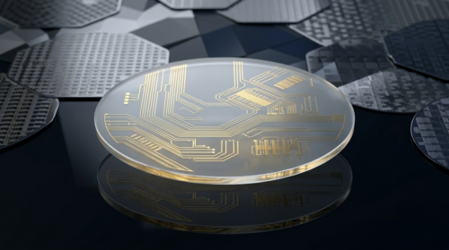
The semiconductor industry is moving towards glass substrates for advanced artificial intelligence (AI) and high-performance computing packages, where conventional organic substrates face limits in supporting larger and denser chiplet designs. Glass offers a more dimensionally stable platform for integrating multiple chiplets and high-bandwidth memory while allowing package dimensions to increase without the same level of warpage and signal-integrity challenges.
Inside an advanced chip package, the substrate sits beneath the silicon dies and provides the fine electrical connections between the dies and the rest of the system. For decades, these substrates have largely used ABF (ajinomoto build-up film), a resin-based organic material that can be compared with the fibreglass-reinforced material used in conventional PCBs, but manufactured to much finer dimensions. As AI accelerators combine processors with multiple high-bandwidth memory (HBM) stacks and chiplets, these organic substrates face increasing limitations. Thermal expansion can cause warpage, while shrinking the spacing between copper interconnects becomes increasingly difficult as more connections are packed into larger packages.
As AI packages have grown beyond 70–100 mm per side to accommodate additional chiplets and HBM stacks, the thermal expansion mismatch between organic substrates and silicon becomes more difficult to manage. The substrate expands and contracts differently from the dies during heating and cooling, increasing the risk of warpage, solder-joint cracking and alignment problems during manufacturing. Organic substrates also face limits in how closely their copper interconnects can be placed, as reducing the spacing to a few micrometres increases electrical interference between neighbouring signals. These constraints make it harder to connect the growing number of chiplets and memory devices required by high-end AI accelerators.
Glass core substrates replace the resin core with a thin panel of specialised glass whose thermal expansion is closer to that of silicon, at around 3 parts per million per degree Celsius. Manufacturers can form thousands of through-glass vias (TGVs) by drilling or laser-etching holes through the panel and filling them with copper to carry power and data between its surfaces. Fine copper wiring can then be built across both sides of the glass. Because glass is more dimensionally stable than organic substrates and can support finer interconnect dimensions, it can accommodate a much higher connection density. Industry estimates suggest glass substrates could support roughly ten times more interconnects in the same area and enable larger packages than conventional organic substrates.

Glass substrates are not yet used in mainstream consumer products. Intel has demonstrated large glass-based packages through its research and development work, while Samsung Electro-Mechanics and LG Innotek have been developing the technology through pilot production. Taiwan Semiconductor Manufacturing Company (TSMC) is also working on glass-panel packaging. The technology is primarily being developed for AI accelerators, high-performance computing systems and data-centre processors, where larger packages and higher interconnect density are increasingly important, rather than for mainstream smartphones or laptops.
Production remains largely at the pilot-line stage in 2026, and scaling the technology presents its own manufacturing challenges. Glass is brittle, so cracks created during drilling, processing or dicing can spread when the panel is exposed to thermal stress, affecting manufacturing yields. The supply chain is also concentrated among a small number of specialty-glass producers, including Corning, AGC, Schott and NEG, which supply high-purity, low-expansion glass suitable for advanced packaging. Establishing additional glass-melting capacity can take years, creating another potential bottleneck as demand for larger AI packages grows.
Limited-volume production of glass core substrates is expected to begin around 2028 for selected high-performance applications, according to a 2026 SEMI and Global Net Corp. industry report. Meanwhile, Counterpoint Research forecasts the combined fan-out panel-level packaging and glass-substrate market to grow from about $650 million in 2024 to more than $8.1 billion by 2030.
India’s semiconductor mission is also building capability in advanced packaging, an area that could become increasingly important as AI accelerator packages grow larger and require higher interconnect density. If India develops packaging expertise around glass substrates while the technology is still maturing globally, it could help the country’s semiconductor ecosystem move beyond chip assembly and testing towards higher-value packaging technologies.
For more information, click here.

