In part 1 of this article, we learnt about LiveWire and Multisim electronic design automation (EDA) tools. Let us now take a look at OrCAD and Proteus.
OrCAD
It is one of the most-popular EDA tools in industry. OrCAD is a suite of tools from Cadence for design, simulation and layout of PCBs. This software is mainly used by design engineers to create electronic schematics and electronic prints for manufacturing PCBs. It enables designing of a circuit from beginning to end. It is highly-customisable; we can alter the components and their characteristics based on our requirements.

It is one of the most-popular EDA tools in industry. OrCAD is a suite of tools from Cadence for design, simulation and layout of PCBs. This software is mainly used by design engineers to create electronic schematics and electronic prints for manufacturing PCBs. It enables designing of a circuit from beginning to end. It is highly-customisable; we can alter the components and their characteristics based on our requirements.
OrCAD comes with three main applications. Capture, the first application, is used to draw a circuit on the screen, known as schematic capture. It offers great flexibility when compared with traditional paper-and-pen drawing, as design changes can be incorporated without difficulty and error corrections can be done easily.
OrCAD comes with three main applications. Capture, the first application, is used to draw a circuit on the screen, known as schematic capture. It offers great flexibility when compared with traditional paper-and-pen drawing, as design changes can be incorporated without difficulty and error corrections can be done easily.
The second application, PSpice, simulates the captured circuit. We can analyse the circuit’s behaviour in different ways and verify that it performs as required.

The second application, PSpice, simulates the captured circuit. We can analyse the circuit’s behaviour in different ways and verify that it performs as required.
PCB Editor, the last, is used to design PCBs. Output of this is a set of files that can be sent to the manufacturer for PCB fabrication or to an electronics workshop. Go through these applications before using any of the tools, as it will improve your learning skills.
PCB Editor, the last, is used to design PCBs. Output of this is a set of files that can be sent to the manufacturer for PCB fabrication or to an electronics workshop. Go through these applications before using any of the tools, as it will improve your learning skills.
The program used here is a version of Simulation Program for Integrated Circuit Engineering (SPICE), which was developed at University of California in Berkeley, USA, in the 1970s. For many years it has been the most-widely-used circuit simulator in the electronics industry. It has many versions, of which we will describe PSpice.
The program used here is a version of Simulation Program for Integrated Circuit Engineering (SPICE), which was developed at University of California in Berkeley, USA, in the 1970s. For many years it has been the most-widely-used circuit simulator in the electronics industry. It has many versions, of which we will describe PSpice.
There are three basic steps to be followed:
1. Draw an electronic circuit using Capture.
2. Simulate it with PSpice using specific models for the devices and analyse its behaviour with Probe.
3. Create basic design steps for the PCB using PCB Editor.
Following are the steps used in OrCAD (16.0 version) for simulation and PCB design:
1. Open OrCAD program on the computer. The file will be in the folder of installed software named OrCAD Capture.
2. Opening the tool will direct you to a Cadence product choice window. Select OrCAD Capture and click OK. It will lead you to a new window of Capture.
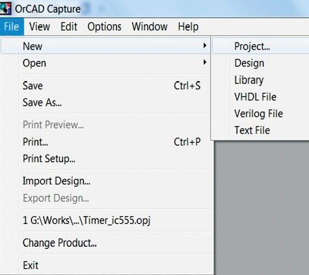
3. Open a new project from File menu (Fig. 12).
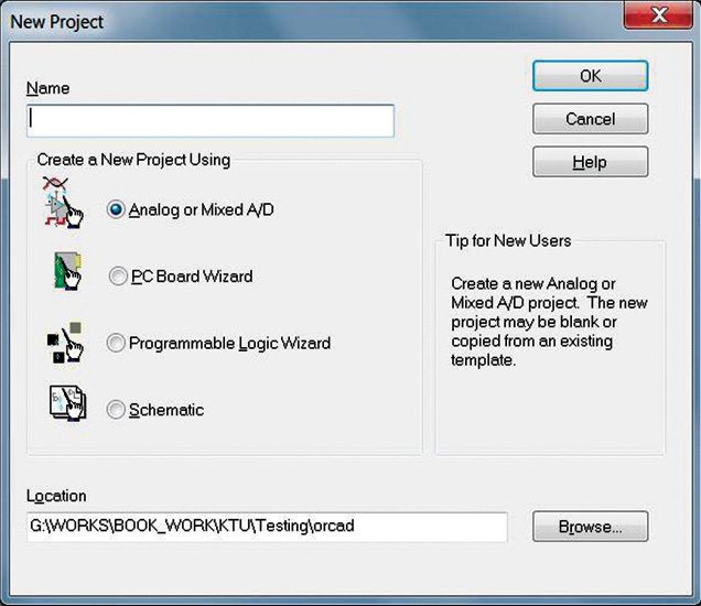
4. Provide the details in the next window and select Analog or Mixed A/D (Fig. 13).
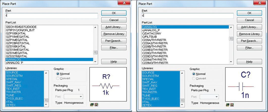
5. Giving project details will lead to a new blank project schematic window. Place the components from option Place→Part. OrCAD library provides a large variety of components. Each component has its own library file. Add those library files to Place Part window using Add Library option.
6. Select the required components from Place Part window. Preview and other details are available in the same window and are visible when the component is selected (Fig. 14). You need to give the exact component name in the part’s place.
7. After placing the components in the schematic, connect the terminals with a wire that can be selected from Place→Wires. Make sure that no parts are left open without connections.
8. Place markers at the corresponding (test) points of circuits where you need to observe the output. For selecting a marker, go to PSpice→Markers→Voltage Level (for voltage reading) as shown in Fig. 15.

9. Simulation can be done by making a simulation profile. It can be done from New Simulation Profile option in PSpice menu. Give a profile name and click Create. This leads to a simulation setting window. We can give customisation for simulation in this window. In this particular example, select Analysis Type Time Domain (Transient). Give sufficient time to run and check Skip The Initial Transient Bias option. After giving inputs, click OK.
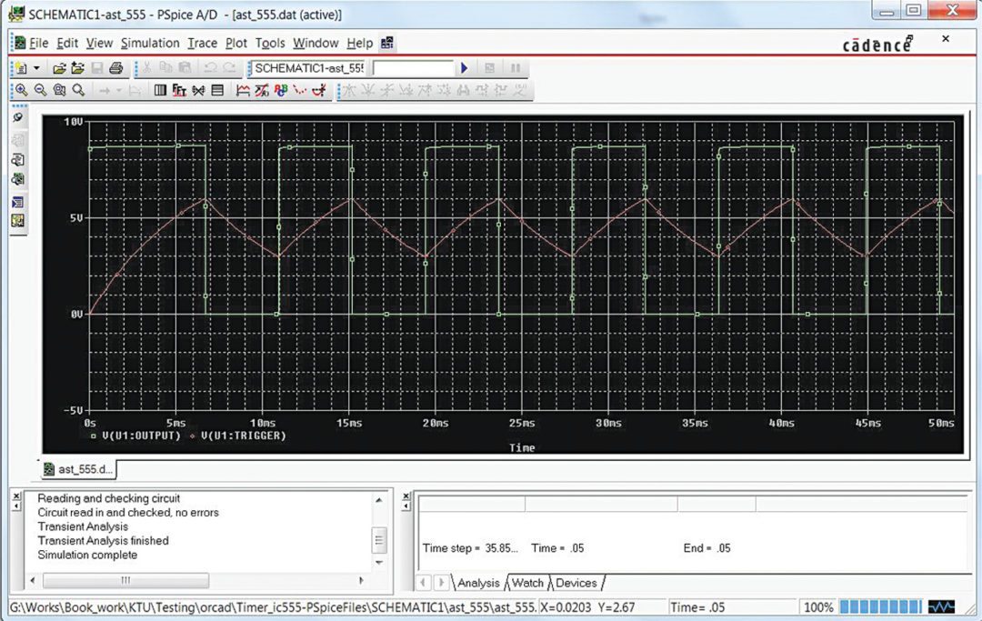
10. Select Run option from PSpice menu and give sufficient inputs. This opens a new simulation window in which you can verify the signals at test points (Fig. 16).
11. Like in all other EDA tools, OrCAD components must also have their own footprint, which is the mechanical outline of the device on the PCB board. Check the property of the device by right-clicking on it. From Property window, check if all devices have their own footprints.
12. Click on your project name on Navigation window (with extension .dsn). Go to Tool→Design Rule Check. Give options as per needs and click OK. This step will check the design for errors, if any, and those will be shown in the log file. Make necessary corrections.
13. Now open PCB Editor from OrCAD folder on your computer. Got to File→New Drawing. Give a proper name and path (preferably in the folder where you created the project) of the file. Select Board Wizard. The wizard will direct you and give sufficient details in the process. Save the drawings.
14. Come back to the schematic OrCAD window and click on your design file. Then, go to Tools option in the menu and click Create Netlist. The programs communicate using files called netlists.
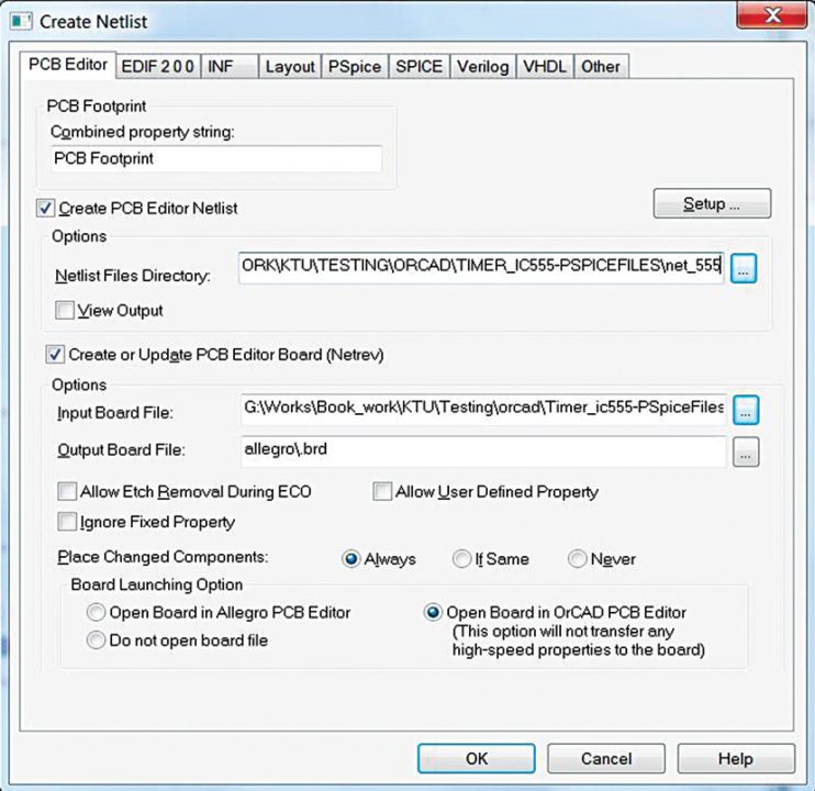
15. A new window will open. Check Create or Update PCB Editor and Create PCB Editor Netlist (Fig. 17). Save the input board file as .brd file that you created and saved in the folder. Give a name for the netlist file. Also, select Open Board option on PCB editor. Click OK.
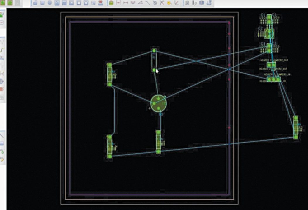
16. PCB editor will automatically open. In Place menu, select Manual option. Now, place all the elements on the side of the rectangular board, and drag and arrange these properly inside the rectangular board place. After arranging the components in a proper manner, without any overlapping, go to Route menu, then PCB router and click on Route Automatic. Routing will be automatically done. You can also do manual routing for better performance (Fig. 18).
17. Go to Manufacture→Artwork. Give the corresponding options. Click on Create Artwork. If you go to the project folder, you will see a file with extension .art. You can print the file also for further manufacturing process.
18. Save your work before closing the window.
Proteus
Proteus ISIS is one of the best simulation software in the world for designing with electronic components including microcontrollers (MCUs). It is a handy tool to test programs and embedded designs. It is a virtual system modelling (VSM) that combines circuit simulation, animated components and microprocessor models to co-simulate complete MCU based designs.
This program allows you to interact with the design using on-screen indicators, LED and LCD displays, and even switches and buttons. One of the main components of Proteus is Circuit Simulation, using which you can simulate programming of the MCU. After simulating your circuit using Proteus software, you can directly make PCB design with it. It is an all-in-one package for designers and hobbyists.
To learn Proteus, you can get plenty of tutorials and video; the more you work on it, the better you become. In this section, we describe Proteus 8 Professional version for simulation. Follow the steps given below:
1. Open Proteus by double-clicking the icon on the desktop or navigating to the installed folder (normally the path is C:\Program Files (x86)\Labcenter Electronics\Proteus 8 Professional\BIN\PDS.EXE). Initially, a Home window will be displayed, which shows recent projects, getting-started tutorials, help, latest news and more.
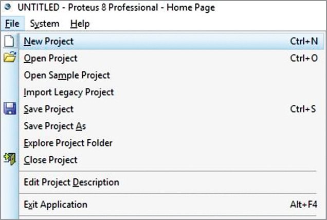
2. To create a new project, go to File→New Project (Fig. 19). It will lead you to New Project Wizard, which helps to create a new project. Give sufficient details like schematic design, PCB layout and firmware. Select default value if you do not know the specifics, or create it later.
3. Finishing the wizard will create a default schematic design just like other EDA tools. Place the components on the schematic window. Placing can be done by selecting Pick Parts From Libraries option in Library menu or by using shortcut key P on the keyboard. This will open Pick Device window.
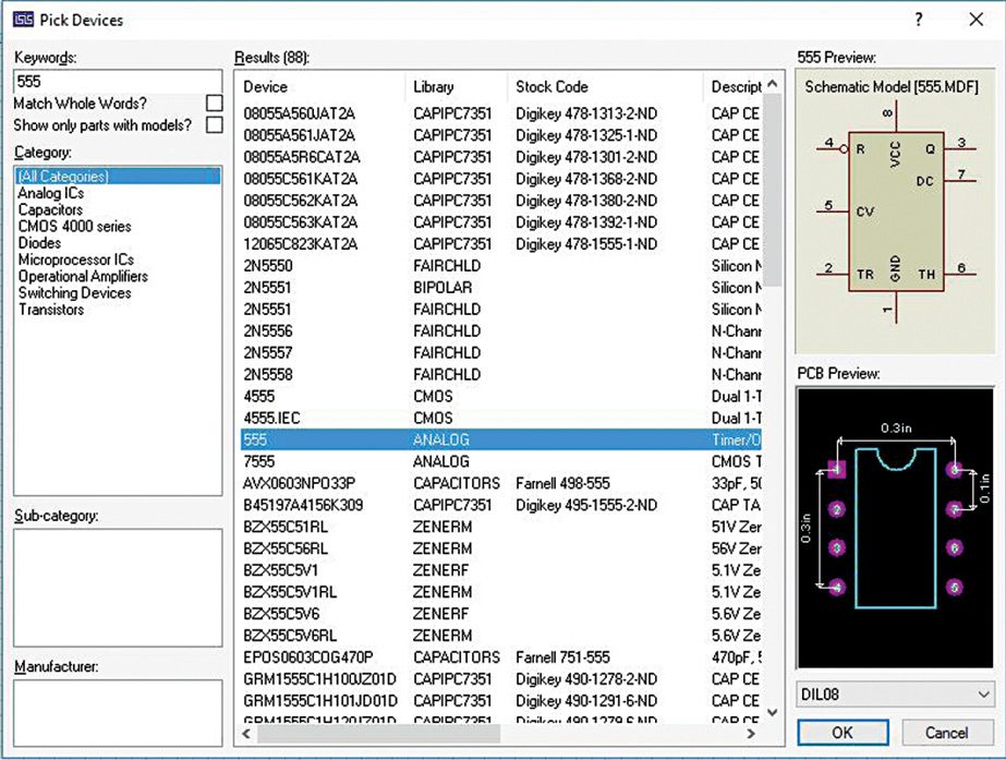
4. From Pick Device window, either search using the keyword or select the component category-wise (Fig. 20). Proteus supports a large variety of electronic components. Selecting each component shows a schematic and PCB preview with other details. Clicking OK will select the device and an image of that device will be shown when the mouse cursor moves over the schematic window. To place device, move the cursor where you want to and click over the schematic. Use Esc key to release selected device.
5. After placing components over the schematic, connect their terminals by clicking-and-dragging technique. Moving the mouse cursor to the terminals will automatically show a pen symbol for drawing the connecting wires. In the left-most corner, multiple modes are present for other activities like component mode, wire label mode, buses mode, sub-circuit mode and more. You can select power supply, ground, input, output, etc from terminal mode. Probe mode is available for using test points, and an oscilloscope is available in instrument section for observing circuit outputs (Fig. 21).
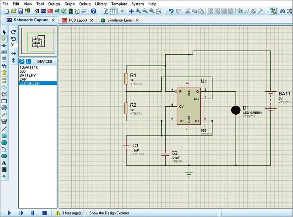
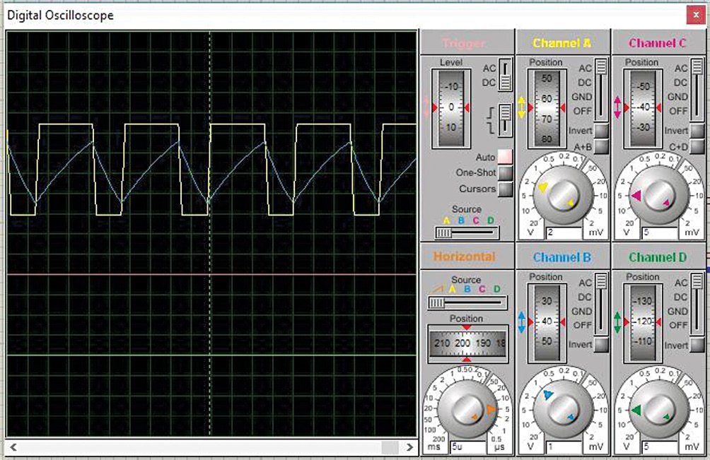
6. Ensure all connections are made and save the project before simulation. To run the circuit, go to Debug→Run Simulation or simply press F12. If you connect an oscilloscope to the circuit while running the simulation, a new digital oscilloscope window will pop up and show the waveforms (Fig. 22).
7. After successful simulation of the circuit, move to the PCB layout. Before going to the PCB design, ensure that all components have their own footprint. Like all other EDA tools, Proteus also has a different tool for PCB design, which is an integrated ARES PCB designing suite. Select Netlist option to ARES from Tools menu; it will open a new PCB layout design window.
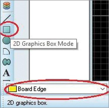
8. Create a board edge. Select 2D Graphics Box Mode in the left corner and select Board Edge from the dropdown list in the left-most corner (Fig. 23).
9. On the workspace, draw a box of sufficient size in which you can place all the components. The circuit should be inside the yellow box; if circuit is complex, you can change the size of the box later.
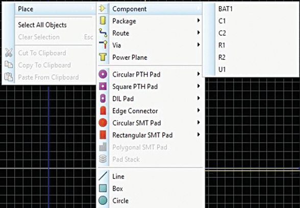
10. Place each component outside the yellow box by right-clicking option Place→Component (Fig. 24).
11. After adding all components to the workspace, arrange the positions of the components properly in the workspace.
12. Next step is tracking, which establishes the connection between components. Connection representation is in green line; yellow line shows direction. After setting track width, click on one end of the component with pen and follow the green line. When two components are successfully connected, the green line will automatically disappear. Multiple PCB layers are also possible in Proteus.
13. In Tool menu, options like auto router and auto placer can also be used by beginners, but manual routing and placing is recommended for better results.
14. To see a 3D image of the final circuit, click on Option 3D Visualization. The PCB layout can be printed from Print Layout option in Output menu.
Manu Prasad is M.Tech in VLSI and embedded systems and is currently working as assistant professor at AWH Engineering College. His interests include VLSI, EDA tools, MATLAB, Latex and so on.