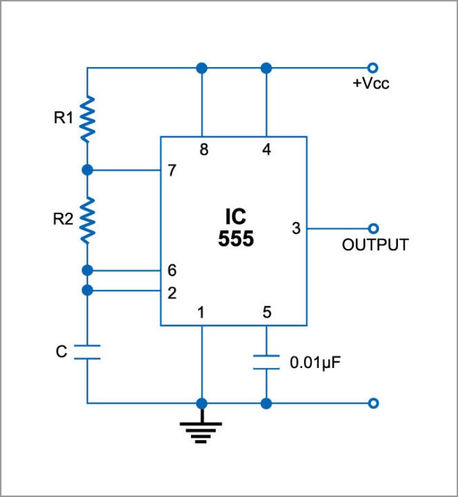
Electronic design automation (EDA) is a software tool used for designing electronic systems. Electronic circuits can be designed and synthesised on a computer using these tools. We can observe the behaviour of the system, analyse it and also get an idea about its cost with these tools, even before its prototype is made. Many EDA tools are available these days, each with their own special functionalities. Most of these are user-friendly, and a knowledge about these could be beneficial both in academic and professional areas. PCB designing, IC designing and testing can also be done with the help of EDA tools. This article introduces you to some of the most-commonly-used EDA tools like LiveWire, Multisim, Proteus and OrCad. Each tool has been explained here by considering a simple astable multivibrator circuit using timer IC 555 (Fig. 1). Each step involved like drawing the circuit, simulating and generating its PCB layout is explained in detail for each of the tools discussed.
LiveWire
LiveWire is a simple, user-friendly EDA tool for the simulation and synthesis of electronic circuits. Circuits can be drawn just by dragging and dropping the components from the tool window and connecting these by joining the nodes. LiveWire comes with an additional tool known as PCB Wizard. We can draw the PCB layout of the circuit with the help of this tool. Automatic placement option can be used for better arrangement of tools and layout.

To demonstrate the implementation of the circuit with this tool, we use LiveWire Professional Edition 1.11 and PCB Wizard Professional Edition 3.50. Install the same on a Windows PC and follow the steps below:
1. Open LiveWire from the desktop by double-clicking on the icon.
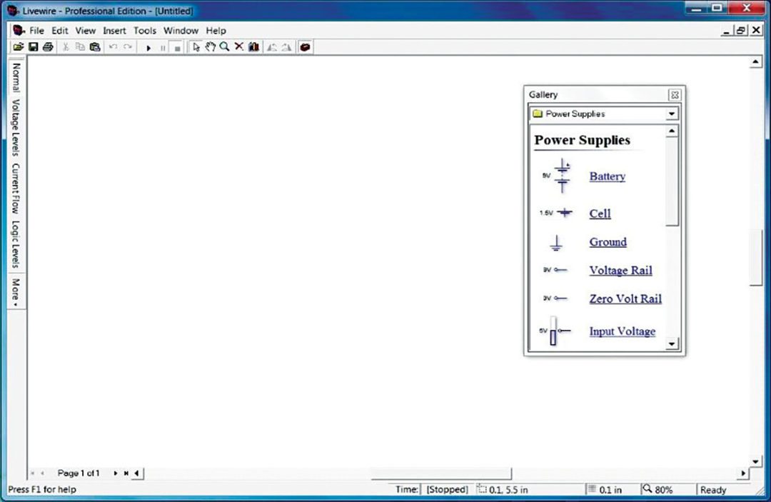
2. A window with a schematic drawing panel and an additional window with the list of components will appear (Fig. 2).

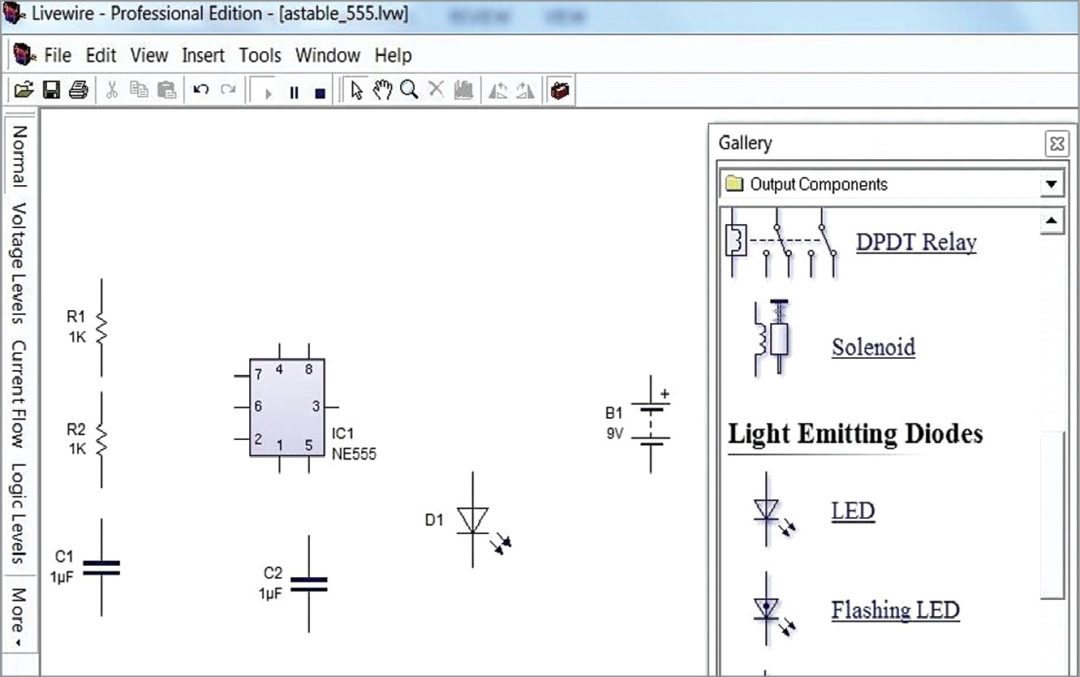
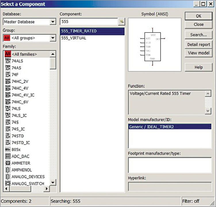
3. With the help of the drop-down list in the component window, select the required components from the list. Just drag and place these in the schematic window as shown in Fig. 3.
The components can be moved and arranged using a mouse and their properties and alignments can be varied with the options obtained by right-clicking on these.
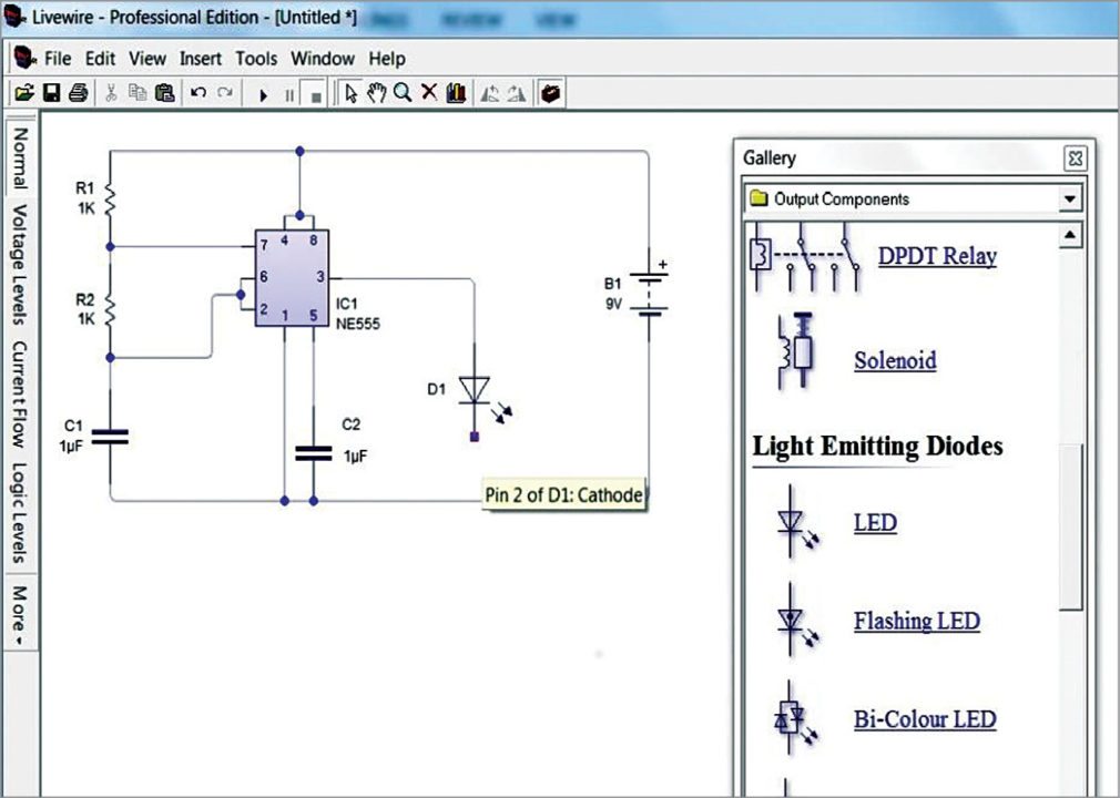
4. After placing the components, connect their terminals as per the circuit. Simply click and drag the mouse pointer between terminals to make the connections (Fig. 4).
5. Save the schematic file in the desired location of the computer. The file will be with extension .lvw
6. Simulate or run the circuit by clicking Run button provided in the standard panel or by simply pressing F9. If some errors are present, these will be intimated in Error window.
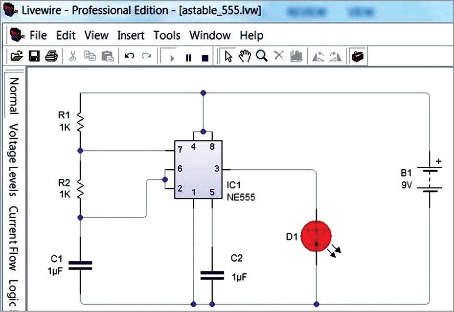
7. Simulation can be verified on the schematic window itself. In this example we use a red LED to verify the result as shown in Fig. 5.
8. For making the PCB layout of the circuit, ensure that the PCB Wizard window is open.
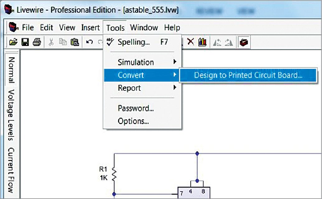
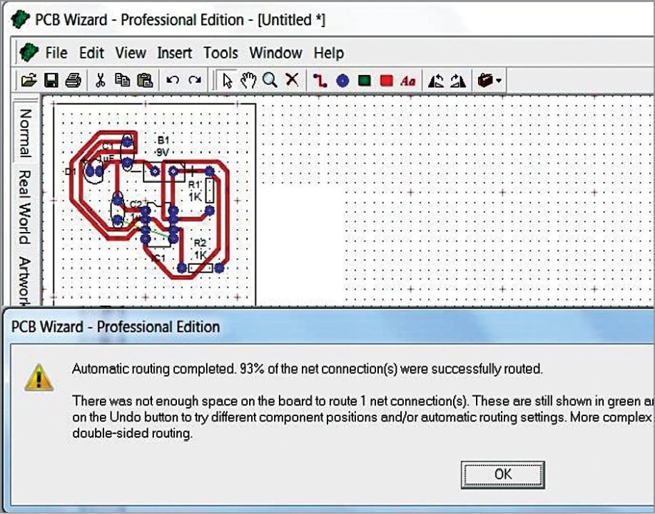
9. Click on Tools option in Menu panel and select Convert Design To PCB option (Fig. 6). PCB Wizard window will open. Give appropriate customisation for a good percentage of routing. If automatic PCB generation does not have sufficient percentage of routing, do the customisation to get a good percentage as shown in Fig. 7. Automatic routing is not always recommended.
10. To take a printout for PCB fabrication, do not forget to take the mirror image of the PCB artwork. For that, go to File menu, click on Mirror PCB artwork in Print option.
Multisim
Multisim is one of the most-commonly-used EDA tools in industries. It supports drawing and simulation of electronic circuits. It provides schematic capture and simulation application of National Instruments Circuit Design Suite, a suite of EDA. Multisim is designed for schematic entry, simulation and feeding to downstage steps such as PCB layout. It also includes mixed analogue/digital simulation capability and microcontroller (MCU) co-simulation.
Ultiboard is used to design PCBs, perform certain basic mechanical CAD operations and prepare these for manufacturing. It also provides automated parts placement and layout. The same circuit used for illustrating the previous section will be used here for familiarising with this software.
Follow the steps given below for drawing and simulating the circuit. Here we use Multisim 12.0 and Ultiboard 12.0 for simulation.
1. Double-click on Multisim icon on the desktop or in the program list. The icon can also be found in the installed folder (normally in C:/Program Files/National Instruments/Circuit Design Suite xx/).
2. As in other EDA tools, a schematic window will open along with a navigation window.
3. Next, place the components in the schematic window by clicking PlaceComponents. This will open a new component window (Fig. 8).
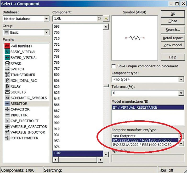
4. From the component window, select the required components. Multisim supports most of the components present in the market. Selecting each component will show the details related to the particular component, like symbol, manufacture, model, footprint and so on.
5. Place the required components on the schematic window and connect each terminal using mouse cursor drag-and-drop technique. Right-clicking options will give other changes like rotation, value of the components and rate.
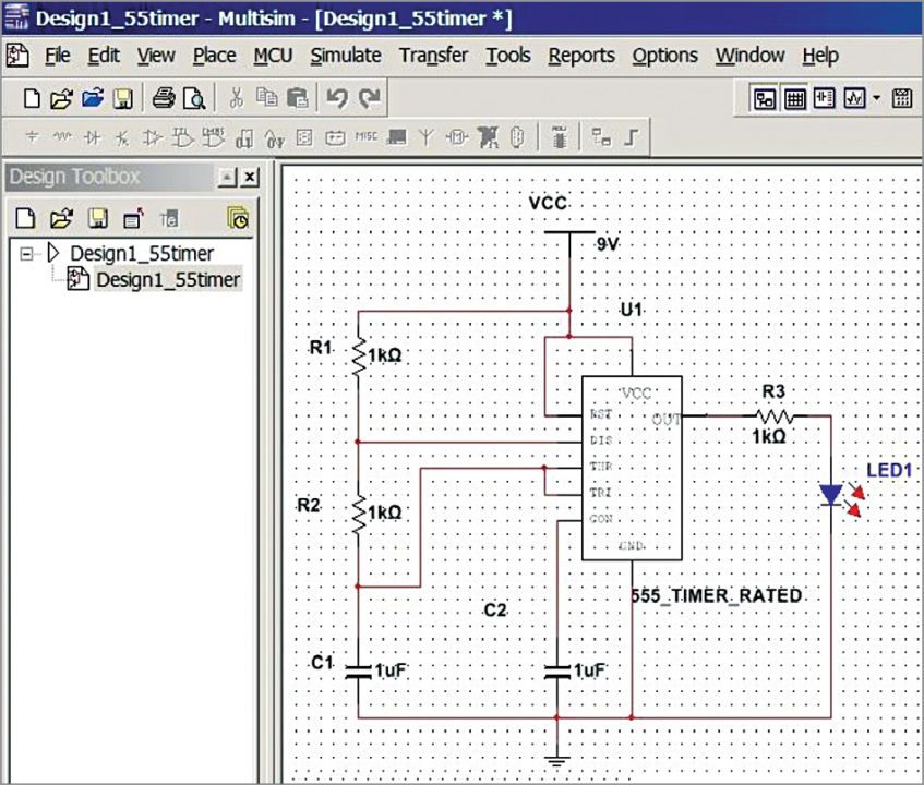
6. After successful connection and parameter entry, simulate the circuit. Before running the circuit, save the project. Then, run the circuit from SimulateRun in the menu (Fig. 9).
7. For PCB design, ensure that each and every component has its own PCB footprint as shown in Fig. 10. (In Multisim, if footprints are available, components will be in blue colour, otherwise these will be in black.) These footprints will ensure the size and pin positions of components. A footprint may vary according to the range and rate variation and even the manufacturer. In Multisim we can create or duplicate a footprint.
8. After confirming the presence of footprint of each component, move to the next tool, Ultiboard, for PCB design. Either open the project file in Ultiboard or go to option TransferTransfer to Ultiboard. Select the file with extension .ewnet and open it.
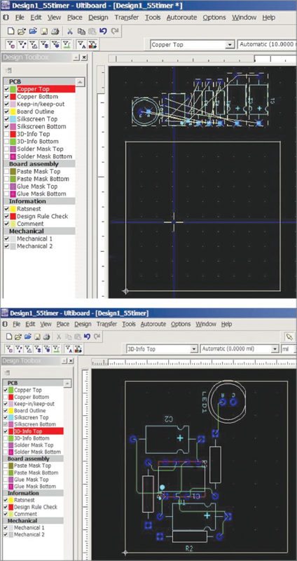
9. The opened black window will show a yellow square and components are placed outside the yellow square. This square is the area of PCB layout whose size can be decided later. Arrange the components in their proper places so that there is good routing (Fig. 11). We can also use the provision of automatic-place-and-routing option from menu AutorouteStart/Resume Autoroute.
To be continued…
Do you like this article? You may also like other software review articles
Manu Prasad is M.Tech in VLSI and embedded systems and is currently working as assistant professor at AWH Engineering College. His interests include VLSI, EDA tools, MATLAB, Latex and so on