The other very exciting aspect of KiCad is that library components for both PCB and schematic are actually plain text files.
KiCad’s principle of use

In order to manage a KiCad project, schematic files, PCB files, supplementary libraries, manufacturing files for photo-tracing, drilling and automatic component placement files, it is recommended to create a project as follows:
1. Create a working directory for the project (using KiCad or by other means).
2. In this directory, use KiCad to create a project file (file with extension .pro) via the ‘Start a new project’ icon.
It is strongly recommended to use the same name for both project files and its directory. KiCad creates a file with a .pro extension that maintains a number of parameters for project management (such as the filename of the principal schematic, list of libraries used in the schematics and PCBs). Default names of both principal schematic and PCB files are derived from the name of the project. Thus, if a project called example.pro was created in a directory called example, the default files will be created as in the ‘Project’ box.
KiCad’s graphical user interface
The main KiCad window (Fig. 1) is composed of a project tree view, a launch pane containing buttons used to run the various software tools and a message window. The menu and the toolbar can be used to create, read and save project files.

KiCad allows you to run all standalone software tools that come with it. The launch pane (Fig. 2) is made of the seven buttons that correspond to the following commands (from left to right): 1 – Eeschema, 2 – Cvpcb, 3 – Pcbnew, 4 – Gerbview, 5 – Bitmap2component, 6 – Pcb calculator, 7 – PI Editor.
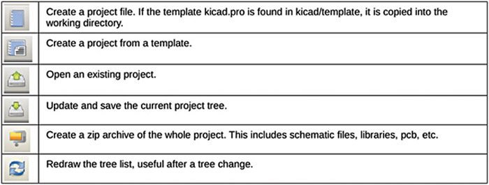
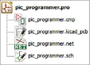
Each project has a project tree view (see Fig. 3). Double-clicking on the Eeschema icons runs the schematic editor, which in this case will open the file ‘pic_programmer.sch.’ Double-clicking on the Pcbnew icon runs the layout editor, in this case opening the file ‘pic_programmer.kicad_pcb.’ Right clicking on any of the files in the project tree allows generic files manipulation. KiCad top toolbar (Fig. 4) allows for some basic files operation (from left to right).
Download and install KiCad
KiCad runs on Linux, Apple OS X and Windows. You can download a copy of KiCad from:
[stextbox id=”grey”]http://kicad.sourceforge.net/wiki/
Main_Page[/stextbox]
Installation instructions are available on the KiCad website under: Info/Install.
Whatever installation method you choose, always go for a recent version of KiCad.
Under Linux. Under Linux, the easiest way to install KiCad is via Aptitude. Type into your terminal:
[stextbox id=”grey”]sudo add-apt-repository ppa:paxer/ppa
sudo aptitude update && sudo aptitude
safe-upgrade
sudo aptitude install KiCadKiCad-
doc-en[/stextbox]
At the time of writing, the standard apt-get repository of Ubuntu offers a version of KiCad which is about one year old. Alternatively, you can download and install a pre-compile version of KiCad, or directly download the source code, compile and install KiCad.
Under Apple OS X. At the time of writing, the best way to install KiCad on Apple OS X was to download a pre-build binary from:
[stextbox id=”grey”]http://kicad.sourceforge.net/wiki/
Downloads[/stextbox]
Note. Installation files for only Linux and Windows platforms are available at Kikad official website.
Note. The latest version of KiCad supports PCBs up to 32 layers.
The author is a senior technical correspondent at EFY. The article has inputs from KiCad’s latest documentation released on March 17, 2014