
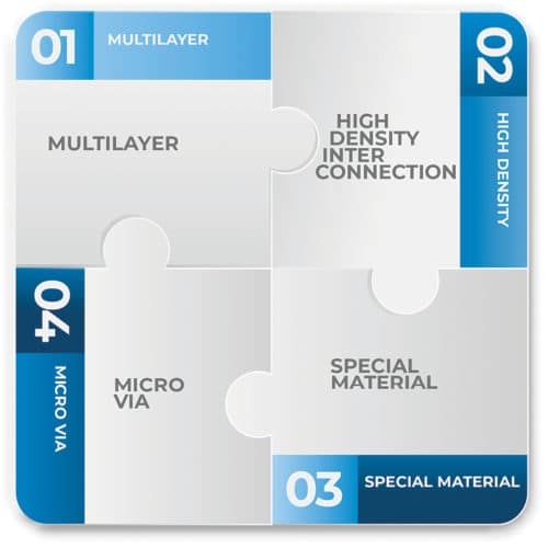
High-density interconnection (HDI) PCB takes advantage of recent technologies to amplify the functionality of circuit boards, motivated by the tininess of parts and semiconductor packages that provide superior characteristics in innovative new products, including touchscreen phones
The first printed circuit board (PCB) can be traced all the way back to the early 1940s. Back then, the US needed basic PCB for military applications. Since then, PCB technology has constantly evolved, from single-sided, double-sided to multilayer, flex, rigid-flex and so on.
For many years, PCB design was dictated by the evolution of components in the quest to provide more efficiency, more capabilities and bigger connection density. The trend is still the same; components continue to decide the evolution of PCB design. Power LEDs are a good example of this.
The same goes for high-density packaging components like ball-grid array (BGA) and micro-BGA. PCB designers have pushed PCB manufacturers to build circuits capable of supporting such fine pitch components.
Engineers, circuit board manufacturers, raw material suppliers and PCB manufacturers have developed processes and laminates to print the design for high-density components. By reducing the pitch, interconnection is getting more and more complex. Vias/holes have to be reduced because pads space has reduced, too.

What is an HDI PCB
HDI stands for high-density interconnection. A circuit board with a higher wiring density per unit area as opposed to a conventional board is called HDI PCB. An HDI PCB has finer spaces and lines, minor vias and capture pads, and higher connection pad density. HDI is the result of component packaging evolution. Most of the new components need PCBs with high density for enhancing electrical performance.
HDI boards are one of the fastest growing technologies in PCB. These contain blind and/or buried vias, and often contain micro-vias that are 0.006 or less in diameter. These have a higher circuitry density than traditional circuit boards.
Now, products do more, weigh less and are physically smaller. Speciality equipment, mini-components and thinner materials have allowed for electronics to shrink in size while expanding in technology, quality and speed.

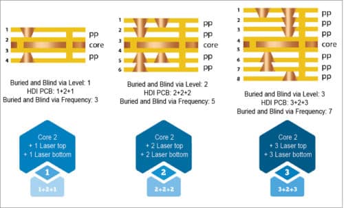
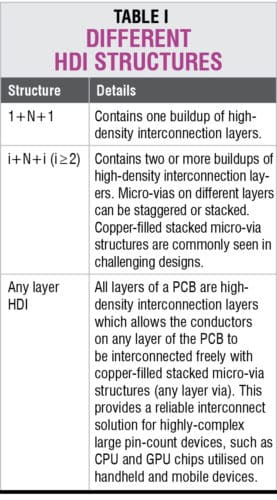
There are different HDI structures:
x + N + x
Here, first x is the number of added layers on the top and bottom sides, N is the initial built-up multilayer (4, 6, 8, … layers) and second x is the number of added layers on the top side.
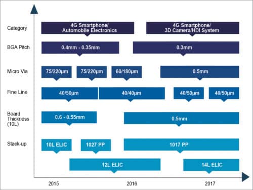
HDI PCB trends and applications
The graph in Fig. 4 shows the trends of HDI development and its main applications.
HDI leads to:
- Line reduction
- Space reduction
- BGA pitch reduction
- Via diameter reduction
- Pre-preg thickness reduction
- Board thickness reduction
- Based copper reduction
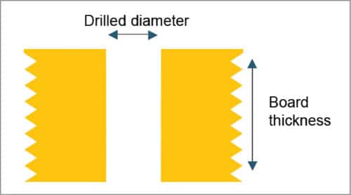
Limitations of HDI PCB are directly linked to plated holes reliability. Limitation of blind via is the aspect ratio. Aspect ratio is the division of material thickness by hole PTH diameter.
The main problem is the plating process. To assume good hole plating integrity, aspect ratio is limited to 1:0.8 for blind vias. Whereas, the advanced value is 1:1.
Due to this aspect ratio limitation, PCB manufacturers select special pre-pregs (very thin, with appropriate reaction to laser drilling). HDI multilayers must be built up with appropriate materials. The standard PP used for standard ML like 7628, 1080 and 2116 is too thick for micro-vias.
Standard pre-pregs contain fibre-glass, which is huge for laser drilling. Glass contained in the pre-pregs changes the laser direction and creates a mediocre or wrong shape quality of laser via holes.
The buildup must use a thinner base copper for good tracks definition. (Many plating processes increase total copper thickness.) The base copper choice also influences the signal propagation for high-frequency applications.
Thinner pre-preg, thinner base copper and thinner PCB are the trends for HDI PCBs.
Via holes are sensitives. Vias are like rivets used during the assembly process. ROHS applies a high thermal stress on vias. Expansion of the material in z-axis stresses the vias. The trend is to continuously reduce via diameter and increase reliability. Further, the assembly process multiplies the number of thermal clocks.
Due to this situation, the only way to reduce the force applied during assembly is to use more stable FR4. Low CTE (coefficient of thermal expansion) materials are mandatory to limit the breaking holes phenomena during the assembly process and in harsh environments.
FR4 Z CTE, alpha 1 and 2, and Tg are the main parameters to follow for material selection. The real challenge is to select the right material, which is also cost-effective. It is important to reduce the total thickness of boards. Reduction of micro-via diameter pushes towards using thinner pre-pregs and laminates.
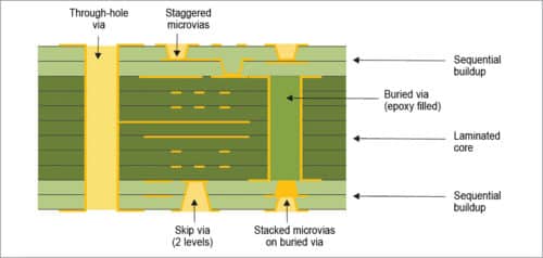
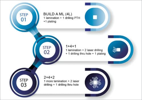
Several laser drillings involve a longer lamination process. The lamination process is shown in Fig. 6.
Laser drilling is a sensitive process. The type of chosen pre-preg (web, laser drillable, etc), method of drilling and aspect ratio must be well-studied to get reliable HDI PCB. The R&D department must analyse these new design constraints carefully. These are detailed below.
CFA phenomena
Right material and layout choice
Via plugging/via filling process
Good design requires clear explanations
Impedance control
DK value, space and lines, dielectric thickness
High-frequency signal propagation in copper
Type of copper versus fine line definition
Advantages of HDI PCB
Advantages of HDI PCBs are given below.
Denser trace routing
It allows incorporation of more components onto smaller boards because HDI PCBs can be populated on both sides of the board.
Enhanced power usage
It decreases power usage, leading to longer battery life in handheld and other battery powered devices.
Smaller weight and size
PCBs fit into little spaces and have a smaller amount of mass than conservative PCB designs. There is lesser chance of harm from mechanical shocks.
Faster signal transmission
A high-density interconnect PCB ultimately results in faster signal transmission along with enhanced signal quality.
Components
It leads to more component space (also by via-in-pad).
Stéphane Barrey is vice president – Europe, and technical director, ICAPE Group


