 Global positioning system (GPS) is a wonderful technology that has made navigation systems highly accurate and efficient in recent years. All the mobile phones these days come with an in-built GPS receiver through which you can easily find out your current location anywhere on the earth. The only thing required is an unobstructed line-of-sight to four or more GPS satellites.
A GPS navigational device is any device that receives GPS signals and processes them to extract information for determining its exact location. Presented here is such a GPS device with a tracking record system. It shows the path traversed by you from the initial position, so you are never lost at unknown locations and can always come back to the initial point.
Circuit and working
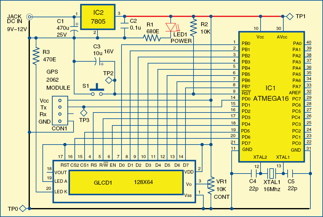
Fig. 2 shows circuit of the GPS navigator. The circuit is built around microcontroller ATmega16 (IC1), 5V voltage regulator 7805 (IC2), GPS module (connected at CON1), graphical LCD (GLCD1) and a few other components.
The circuit is powered by a 9V/12V adaptor. Regulator IC2 provides 5V regulated supply for the circuit to operate. LED1 indicates presence of power in the circuit.
Microcontroller IC1 running at a clock frequency of 16 MHz communicates with the GPS receiver modem via serial protocol. Tx pin of the GPS receiver is connected to Rx (PD0) pin of microcontroller IC1. The GPS receiver continuously transmits data at 1Hz update rate.
A 128×64-pixel, KS0108-controller-based GLCD is used to display the navigation data. Port pins PB0 through PB7 of IC1 are connected to data pins D0 through D7 of GLCD1. Port pins PD2 through PD6 are used to provide control signals RS, R/W, EN, CS1 and CS2 to GLCD1, respectively. Switch S1 is used to reset the navigator.
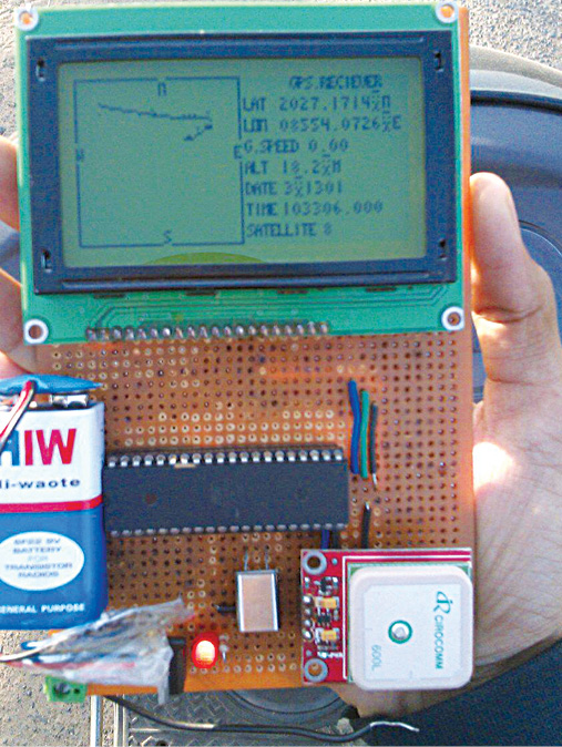
Working of the navigator is simple. Once powered on, the microcontroller stores the initial longitude and latitude data. Then it continuously plots the changing latitude and longitude as you move around (refer Fig. 1). One division change on the screen is equivalent to approximately 30 metres travelled. With the new latitude and longitude position plotted on the screen, you get a clear idea of the direction and path traveled by you. The display also shows various other information such as current latitude, longitude, speed, altitude, date, time and number of satellites the GPS modem can capture.
Software
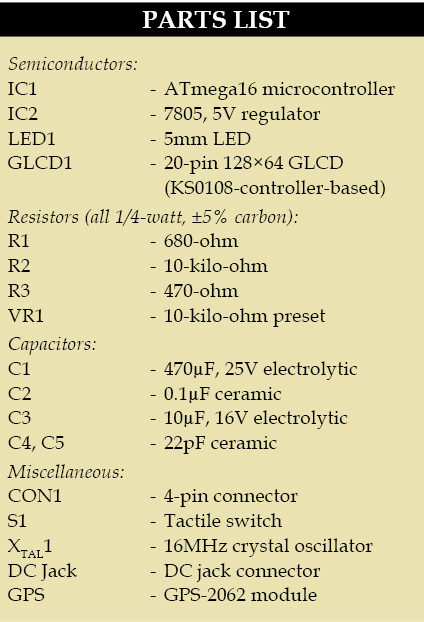
The software program is written in ‘C’ language and compiled in WINAVR Programmers Notepad. WINAVR is a GCC–based compiler for AVR. Burn the program into the MCU using a suitable programmer with FUSE BYTE settings mentioned below:
L fuse-0xef
H fuse-0x99
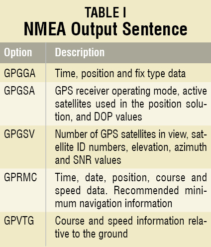
The GPS receiver modem continuously sends data via USART to IC1 at 9600 baud rate. GPS data is initiated by a ‘$’ sign followed by National Marine Electronics Association (NMEA) output sentences. Details are given in Table I.
The microcontroller continuously captures and stores all bytes for each NMEA output sequence. The total bytes are then partitioned and sampled into a small packet containing information about time, date, longitude, latitude, altitude, speed, etc. These values are regularly updated and displayed on the GLCD.
Download Source Code: click here
Construction and testing
An actual-size, single-side PCB for the GPS navigator circuit is shown in Fig. 3 and its component layout in Fig. 4. Assemble the circuit on the provided PCB to minimise assembly errors. Use IC base for microcontroller IC1. You can use a 9V/12V adaptor or any other suitable DC source to power the circuit.
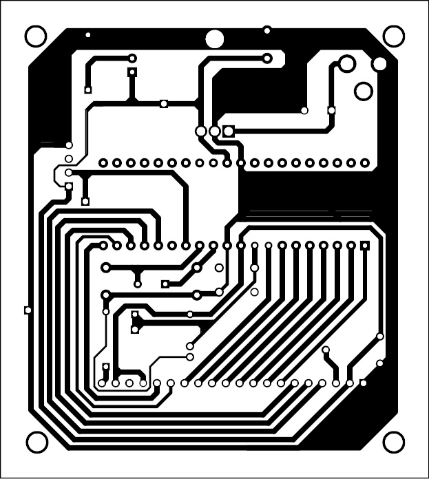
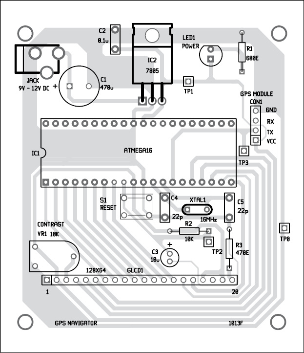
Download PCB and Component Layout PDFs: Click here
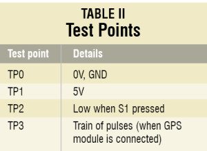
To test the circuit for proper functioning, verify 5V power supply at TP1 with respect to TP0. Reset to the system can be checked at TP2. The data transmitted by the GPS modem can be observed at TP3 using an oscilloscope.
The author is a third-year B.Tech student of electrical engineering from the College of Engineering & Technology, Bhubaneshwar.


Sir ,
Please give me source code into pdf formet
my mail id is [email protected].
Your project is awesome.
Dear Ashu, the source code is present within the article.
Hello
The exe source code does not correspond to an exe code
with which program you compile it I don’t understand
Please excuse my ignorance in this area or I start
I find this work remarkable and I would like to carry out your system to be able to try it
if you can give me the instructions to carry out this programming
I would be happy to you
Thank you
Hola.
No puedo descargar código fuente.
Pantalla, 404 error.
Donde puedo encontrarlo?
[email protected]
El código fuente no es necesario para este artículo.