


 A light-dependent resistor (LDR) whose resistance is inversely proportional to the intensity of light is often used as a sensor in electronic projects that involve the use of light. This project uses an LDR to control the speed of a DC motor.
Most outdoor LED displays and some indoor LED displays are built around individually mounted LEDs. Presented here is a LED scrolling display that uses 64 LEDs to display alphabets and numbers. A cluster of red, green and blue diodes is driven together to form a full-colour display.
In a dot-matrix LED display, the LEDs are wired together in rows and columns to minimise the number of pins required to drive them. For example, an 8×8 matrix of LEDs, shown in Fig. 1, would need 64 I/O pins—one for each LED pixel. By wiring all anodes together in rows (R1 through R8) and cathodes in columns (C1 through C8), the required number of I/O pins is reduced to 16.

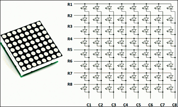
Each LED is addressed by its row and column number. In Fig. 1, if R4 is pulled high and C3 is pulled low, the LED in the fourth row and third column will turn on. Alphabets and numerals can be displayed by fast scanning of either rows or columns. In this project, column scanning has been used.
Working of a dot-matrix display
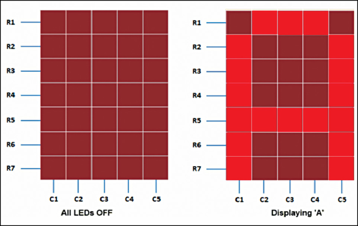
Fig. 2 shows which LEDs in a 5×7 matrix of LEDs are to be turned on to display the English alphabet A. The seven rows and five columns of the array are controlled through a microcontroller.

If we want to display alphabet A, we will first select column C1 (which means C1 is pulled low in this case) and deselect other columns by blocking their ground paths (one way of doing that is by pulling C2 through C5 pins to logic high). Now, the first column is active, and you need to turn on the LEDs in rows R2 through R7 of this column, which can be done by applying forward-bias voltages to these rows.

Next, select column C2 (and deselect all other columns) and apply forward-bias voltages to resistors R1 and R5, and similarly for columns C3 and C4. Then, activate column C5 by pulling it down and deselect other columns, and apply forward-bias voltages to LEDs in rows R2 through R7.
By repeating these steps quickly (>100 times per second), and turning on the respective LEDs in each row of that column, the persistence of vision comes into play and we perceive the displayed image of the alphabet A as still.
You must have noticed that across each row one pin is sourcing the current for only one LED at a time, but a column pin may have to sink the currents from more than one LED. For example, column C1 should be able to sink the current from six LEDs while displaying alphabet A. A microcontroller has low sourcing as well as sinking capabilities. To obviate this limitation, external transistor arrays or buffers are used. In this project, PNP transistor BC558 (T1-T8) has been used for this purpose. In the circuit, an 8×8 dot-matrix has been used.
A brief description of the ICs used
IC1 is a 7805, 5V regulator IC, which provides the 5V output voltage for driving the circuit around microcontroller IC2. AT89C52 (IC2) is a low-power, high-performance CMOS 8-bit microcontroller. It has 8k bytes of Flash ROM, 256 bytes of RAM, 32 I/O lines, three 16-bit timers/counters, a six-vector two-level interrupt, a full duplex serial port, an on-chip oscillator and on-clock circuitry.
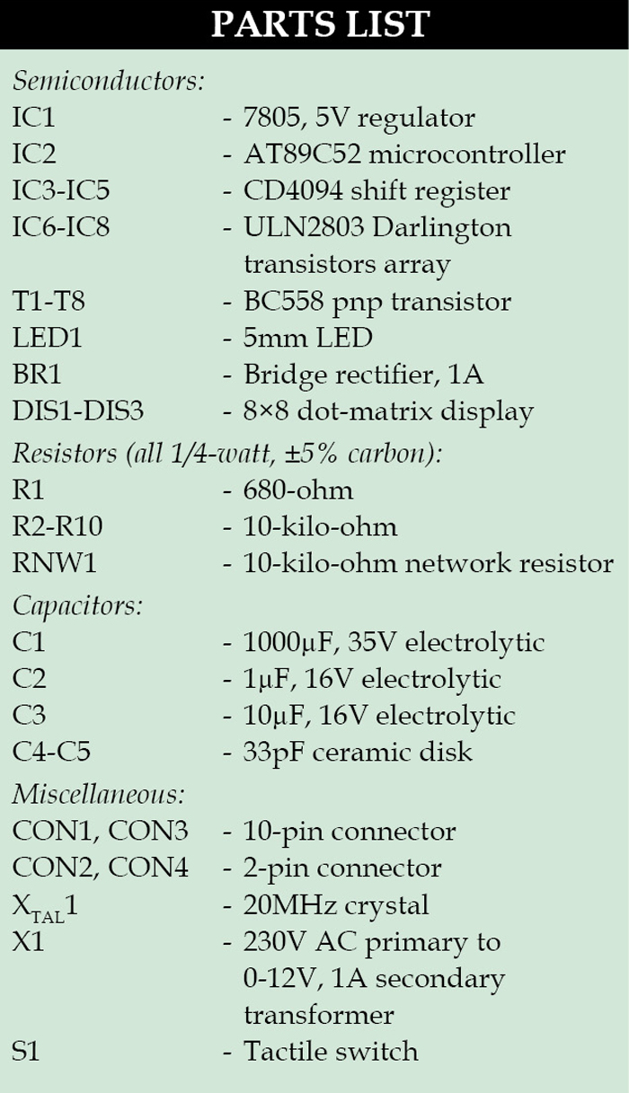 CD4094 (IC3-IC5) is an 8-stage serial shift register, having a storage latch associated with each stage for stroking data from the serial input to parallel buffered 3-state outputs. The parallel outputs may be connected directly to common bus lines. Data is shifted on positive clock transition. Data in each shift register stage is transferred to the storage register when the strobe input is high. Data in the storage register appears at the outputs, whenever the Output-Enable signal is high. Two serial outputs are available for cascading a number of CD4094 devices.
Data is available at the Q serial output terminals on positive clock edges to allow for high-speed operation in cascaded system. The same serial information, available at the Q terminals on the next negative clock edge, provides a means for cascading CD4094 devices when the clock rise time is slow.
ULN2803 (IC6–IC8) is an octal high-voltage, high-current Darlington transistor array. The eight NPN Darlington connected transistors (T1-T8) are ideally suited for interfacing between low-logic-level digital circuitry and the higher current/voltage requirements of lamps and relays. The device features open-collector outputs and freewheeling clamp diodes for transient suppression. It is designed to be compatible with standard TTL families of Ics.
LED scrolling display circuit and working
The circuit diagram is divided here into two parts. The first part has a power supply and controller circuit as shown in Fig. 3. The display unit is in the second part as shown in Fig. 4.
The power supply circuit is built around a step-down transformer, bridge rectifier and 5V regulator. The configuration is conventional. The circuit provides regulated 5V for operation of the circuit.
Microcontroller AT89C52 provides outputs to control the logic levels for the eight rows R0-R7 through port A (P0.0-P0.7). RNW1 is a network resistor, which acts as a pull-up resistor for port 0. An array of eight pnp BC558 transistors (T1-T8) working as current drivers takes care of the current required for LEDs of the dot-matrix; the microcontroller has low sourcing capabilities. The reset arrangement is made at pin 9 of the microcontroller with the help of capacitor C3, resistor R2 and switch S1.
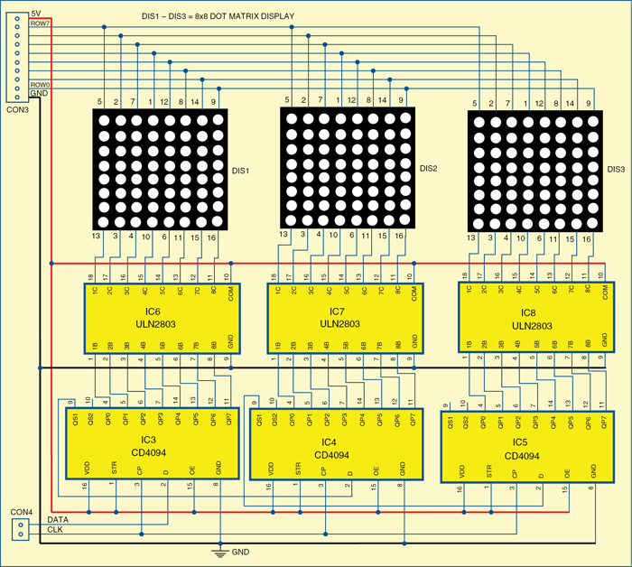
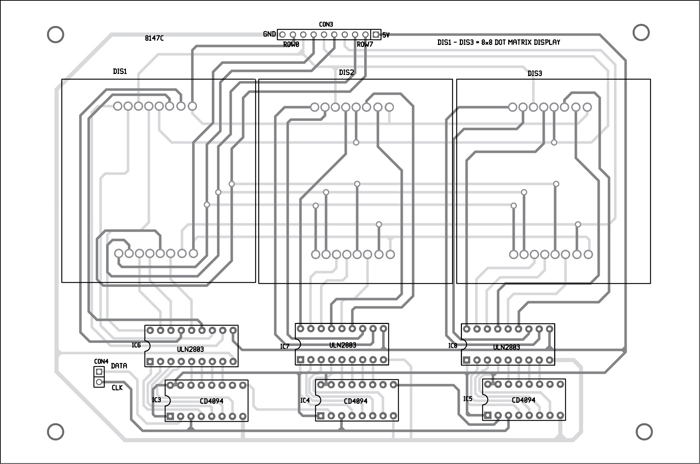
The circuit for the display unit is shown in Fig. 4. It is built around three CD4094 cascaded 8-bit shift registers (IC3-IC5), three ULN2803 high-current Darlington transistor arrays (IC6-IC8) and three 8×8 dot-matrix displays (DIS1-DIS3). Clock and data pulses are generated by the microcontroller at ports P2.1 and P2.0, respectively. These are transferred to the display unit through connectors CON2 and CON4.
Download PCB and component layout PDFs: click here
Download source code: click here
Clock pulses are fed to pin 3 of all the three shift registers, while data pulses are fed to pin 2 of the first shift register, IC3. The output of the first shift register from pin 9 is fed to pin 2 of the second shift register, IC4. To complete the cascading, output of the second shift register from its pin 9 is fed to pin 2 of the third shift register, IC5.
Data from the shift registers is used for activation or deactivation of columns of the three dot-matrix displays (DIS1-DIS3) through IC6-IC8 ICs. For controlling the logic levels at rows R0-R7, data from port P0 is transferred from the microcontroller to the display unit through connectors CON1 and CON3, with a supply of 5V and common ground to display unit of these two connectors.
Software
The source program for the LED scrolling display of ‘EFY INDIA’ is written in Assembly language and compiled using Keil μVision4 compiler. The generated hex code is burnt into the microcontroller using a suitable programmer.
Construction and testing of LED scrolling display
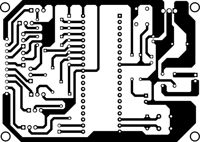
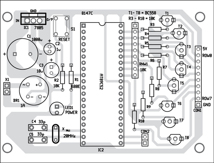
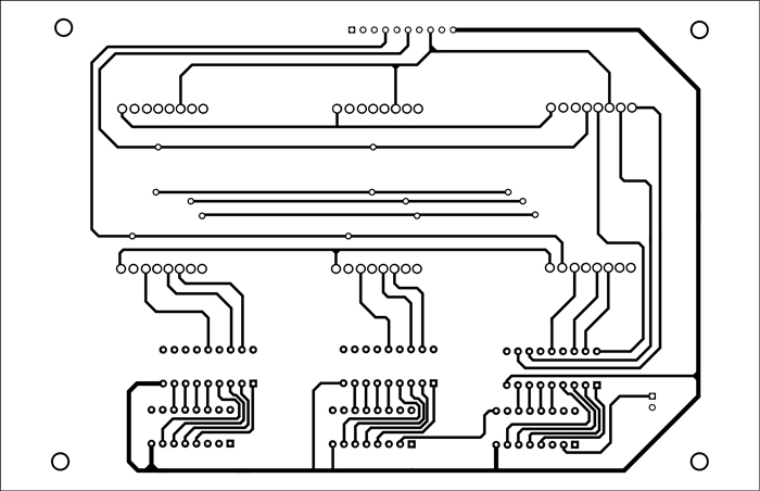
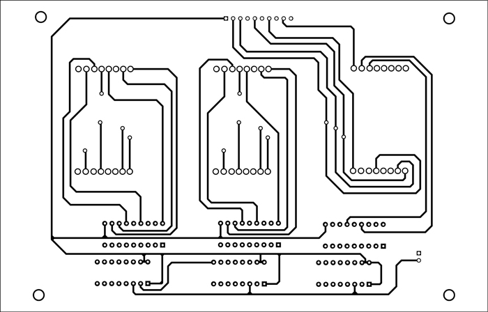
A single-layer PCB layout for the power supply and the microcontroller unit is shown in Fig. 5 and its component layout in Fig. 6. PCB for the display unit is a double-sided one. Track layout of its bottom layer is shown in Fig. 7 and of top layer in Fig. 8. Component and track layouts of the top layer as well as the bottom layer are shown in Fig. 9.
Assemble the circuits on the PCBs to save time and avoid assembly errors.
Harwinder Singh is a project associate in DECD at C-DAC, Mohali, Punjab
This LED scrolling display circuit was first published on 21 September 2016 and was recently updated on 22 January 2019.


What is the maximum limit on the number of displays ( 8*8 LED display) we can use with this circuit.
but we want the scrollin display of 4 meteres length and 2m height
I dont open its program plz send it to my E mail id
[email protected]
Download the code from here: http://efymag.com/admin/issuepdf/LED_Scrolling_Display.rar
Plz send new codes
in embaded c program for scrolling led display
microcontroller at89c52
and plz din’t send old codes those does not open
This code is not suitable for this schematic diagram of fig. 3:. this code is working with your attached proteus project. If I use UNL2803 in proteus it is not working because its NPN type and need +ve volt to its input but Iam getting -ve form shift register CD4094 . And also getting +ve from P0.
Please provide a new code for the schematic diagram of fig. 3:.
Thanks:
This code is working for 3 nos 8×8 dot matrix scrolling display . I have modified the hardware by increasing another 3 nos of dot matrix (total 6 nos) by adding 3 nos of shift register in series. And I think there is no error in hardware but unfortunately I have no idea to modify .asm code to fit for the new 6nos 8×8 dot matrix display.
The display is working but like a parallel display (like duplicate copy). If I display “WELCOME” , it is displaying “W E L W E L” instead ” W E L C O M E” . It start from both 6th and 3rd matrix and not merging all over the matrix .
Scrolling from 6th to 4th and another scrolling from 3rd to 1st matrix
please help me to modify the code.
I need all parts pls give the rate of packade excluding led matrix i make it self.can you also provide the modification of programme and ckt also for 6(8*8)matrix
What modifications need to be done to make the circuit display message based on input from an ir transmitter
Please provide Component layout of dot matrix display and ic unit
Good day to you all please let’s create a WhatsApp group forelectronicsforu.com my phone number is +2347035557795
Sorry, we could not allow you to create a Whatsapp group for our website.
As of now, there is no WhatsApp group for Electronics For You. Will let you know once it is there.
good day sir.please can i have the complete code for the scrolling message.i wish to build the circuit
The complete code is present on the second page.
is there any program required for scrolling data in this system . if it is how to program that data and where it resides that program data.send me
Nicely explained
Thanks for the feedback!
Kindly help with code in C
We do not have C program for this project, sorry.
Hi,
can you please share the code of this project .I need a reference if yo don’t mine.
Please mail the code
can you send me code and diagram of led scrolling display 12 hr or 24 hr digital clock using 8051 or avr (any one micro controller) [email protected]
Hi, I loved your project, but there were a couple of things I didn’t understand. How can I change the message?
NICE PROJECT, BUT PLEASE I WANT TO INCREASE THE NUMBER OF THE 8X8 LED MATRIX FROM 3 TO 8, WHAT SHOULD I DO.
Thanks for the feedback! To add more LED matrix, you can increase hardware such as shift registers and transistor arrays as shown but you also need to slightly tune the software.
sir.plac code
Kindly refresh the page.
please send me the source code
Sent on your email ID.