


 Here we describe how to control electrical and electronic gadgets from a remote location using radio frequency (RF) transmission. An RF interface is used instead of infrared (IR) to avoid the drawbacks of an IR interface. Besides, RF has a longer range. The signal is transmitted by an RF transmitter and received by an RF receiver to switch on or switch off the desired device. This system can be used to control up to fifteen devices.
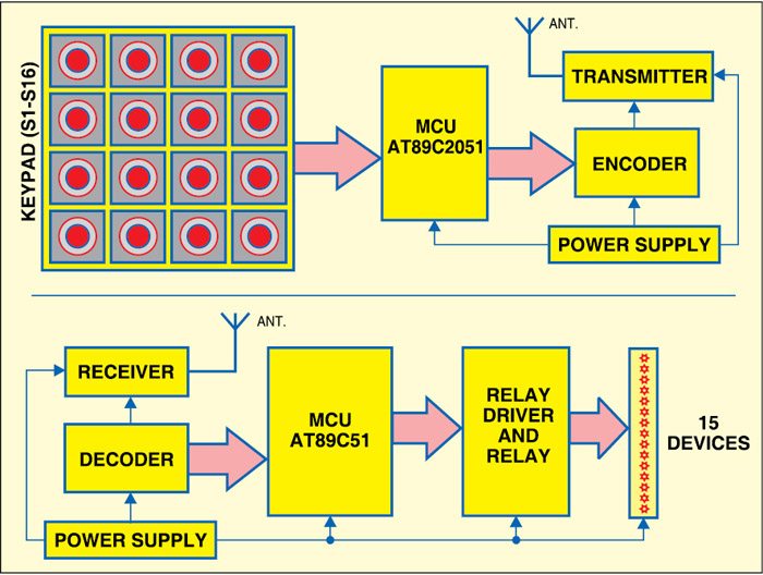
Fig. 1 shows the block diagram for RF-based multiple device control using microcontroller. Signals from the keypad are fed to microcontroller AT89C2051, which, in turn, is interfaced to the RF transmitter through encoder HT12E. The microcontroller continuously reads the status of the keys on the keypad.
When any key is pressed, data is passed to the encoder and then to the RF transmitter from where it is transmitted. The RF receiver receives this data and gives it to the RF decoder. The decoder serially converts the serial bit data into four-bit data at a port of microcontroller AT89C51. The microcontroller energises the corresponding relay through a relay driver. Devices are connected to normally-open (N/O) contacts of the relays.

HT12E and HT12D
HT12E and HT12D are CMOS ICs with a working voltage range of 2.4V to 12V. Encoder HT12E has eight address lines and four address/data lines. The data set on these twelve lines (address and address/data lines) is serially transmitted when transmit-enable TE pin (pin 14) is low. The data output appears serially on DOUT pin. Data is transmitted four times in succession.
The frequency of the pulses of data transmission may lie between 1.5 kHz and 7 kHz depending on the resistor value used between oscillator pins 15 and 16.
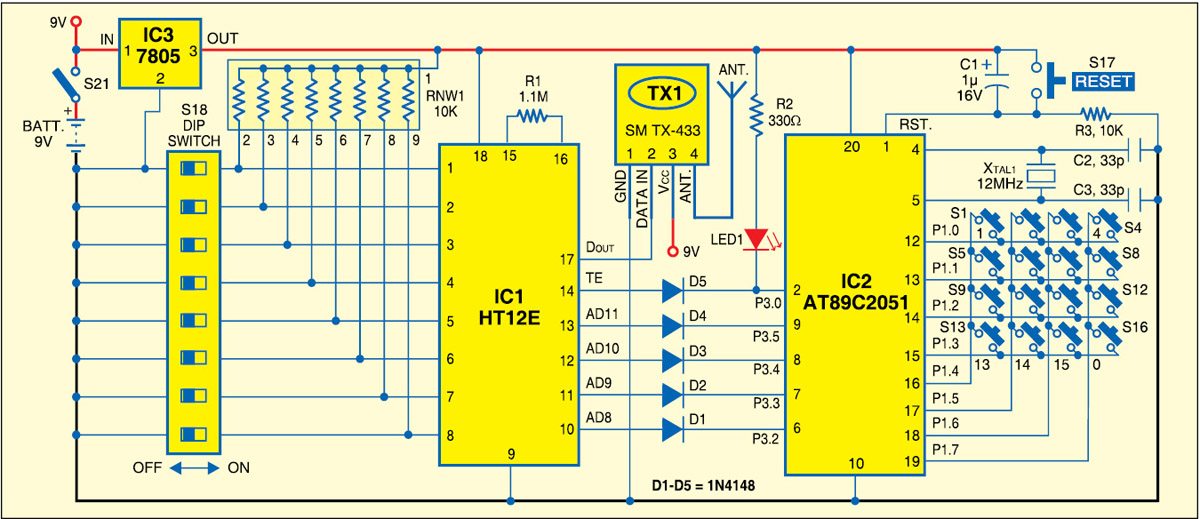
 The internal oscillator frequency of decoder HT12D is 50 times the oscillator frequency of encoder HT12E. The values of timing resistors connected between pins 15 and 16 of HT12E and HT12D, for the given supply voltages, can be determined from the graphs given in the datasheet of the respective chips. The resistor values used in the circuit here are chosen for approximately 3kHz frequency for encoder HT12E and 150 kHz for decoder HT12D at a VDD of 5V.
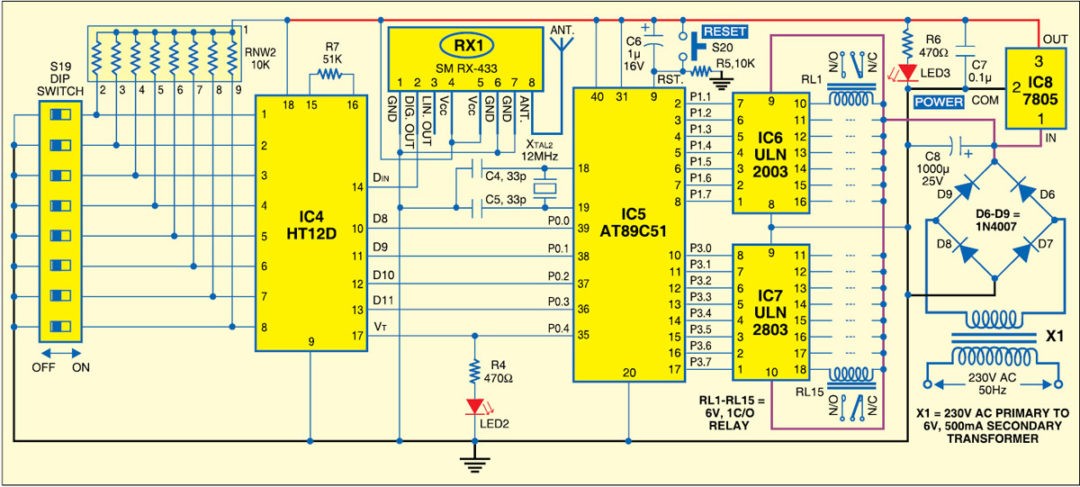
Decoder HT12D receives data from HT12E on its DIN pin serially. If the transmitted address matches the address of the decoder four times in succession, valid transmission pin (VT) becomes high. The data from pins AD8 through AD11 of the HT12E appears on pins D8 through D11 of the HT12D.
Transmitter unit
Fig. 2 shows the transmitter circuit with SM TX-433 RF module (TX1). TX1 is an AM/ASK transmitter module operating at 433 MHz. AT89C2051 is a low-voltage, high-performance CMOS 8-bit microcontroller. It has 2 kB of Flash, 128 bytes of RAM, 15 input/output (I/O) lines, two 16-bit timers/counters, a five-vector two-level interrupt architecture, a full-duplex serial port, a precision analogue comparator, on-chip oscillator and clock circuitry.
Power-on reset is provided by the combination of resistor R3 and capacitor C1. Switch S17 is used for manual reset. A 12MHz crystal along with two 33pF capacitors provides the basic clock frequency for operation.
The receiver address to be transmitted can be set with the help of 8-way DIP switch S18. Port pins P1.0 through P1.7 of the microcontroller are interfaced with the keypad. Pins P3.0 and P3.2 through P3.5 are interfaced with TE pin and data inputs AD8 through AD11 of encoder HT12E.
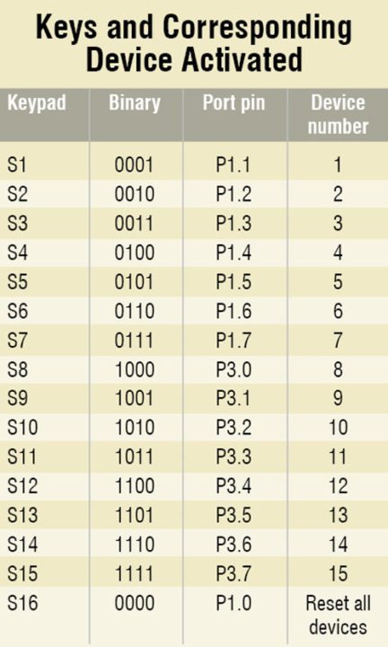 When all switches (S1 through S16) are opened on the keypad, the microcontroller pulls the TE pin as well as data input pins AD8 through AD11 to logic 1. If any switch is closed, the microcontroller pulls the corresponding data pin along with TE pin to logic 0. When switch S1 is closed, the microcontroller makes pin 10 (AD8) and pin 14 (TE) of encoder HT12E low, and logic 0 is transmitted through TX1. The other data pins of encoder HT12E will be in logic 1 state in this case. LED1 glows to indicate transmission enabled.
Receiver unit
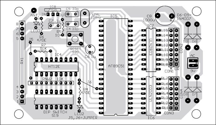
Fig. 3 shows the receiver circuit with SM RX-433 RF module. AT89C51 is a low-power, high-performance CMOS 8-bit microcontroller. It has 4 kB of Flash, 128 bytes of RAM, 32 I/O lines, two 16-bit timers/counters, five-vector two-level interrupt architecture, a full-duplex serial port, on-chip oscillator and clock circuitry.
Power-on reset is provided by the combination of resistor R5 and capacitor C6. Switch S20 is used for manual reset. A 12MHz crystal along with two 33pF capacitors provides the basic clock frequency to microcontroller AT89C51.
Address lines of the encoder (IC1) and the decoder (IC4) should be identical for data reception in the receiver. Here addresses are made identical through switches S18 and S19. When any of the keys on the keypad is closed, the corresponding data pin of the decoder goes low. When any data is received, valid transmission pin (VT) goes high as indicated by LED2.
Data outputs D8 through D11 of HT12D are connected to port pins P0.0 through P0.3 of the microcontroller. The microcontroller receives the decoded data and controls the corresponding relay through relay drivers ULN2003 and ULN2803. The device to be controlled is connected to the relay contacts. Unregulated power supply is used for relays.
Power supply
The 230V AC mains is stepped down by transformer X1 to deliver a secondary output of 6V, 500 mA. The transformer output is rectified by a full-wave rectifier comprising diodes D6 through D9, filtered by capacitor C8 and regulated by IC 7805 (IC8). Capacitor C7 bypasses the ripples present in the regulated supply. LED3 acts as the power indicator and R6 limits the current through LED3.
Software
Programs for the microcontrollers are written in BASIC and compiled using BASCOM Basic compiler for 8051 family. These are supported by Windows OS. The microcontrollers of the transmitter and receiver units are programmed with source programs ‘Remote.bas’ and ‘Receiver.bas,’ respectively. The bas codes are converted into hex codes using the above compiler. The hex codes are burnt into the respective microcontrollers using a suitable programmer.
Download Source Code for Multiple Device Control System: click here
Construction and testing
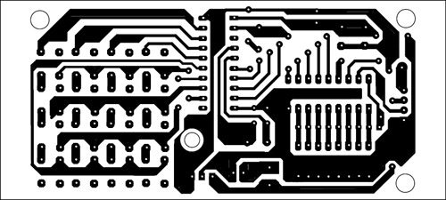
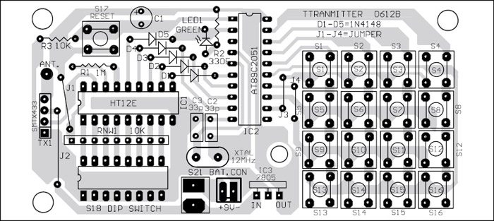
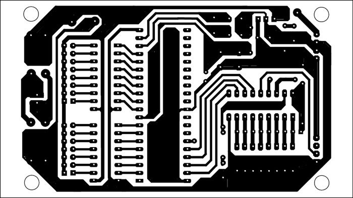
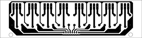
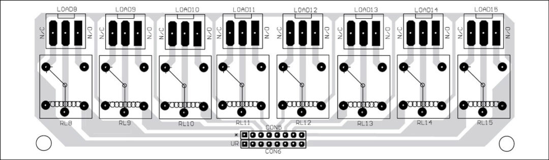
A single-side PCB for the transmitter circuit (Fig. 2) is shown in Fig. 4 and its component layout in Fig. 5. The PCB for the receiver circuit excluding relay section (Fig. 3) is shown in Fig. 6 and its component layout in Fig. 7. The PCB for relays RL8 through RL15 connected to load 8 through load 15 is shown in Fig. 8 and its component layout in Fig. 9. You can use another PCB for relays RL1 through RL7 to connect load 1 through load 7. Suitable connectors are provided on the PCB. The receiver PCB is interfaced with the relay PCB by connecting CON1 to CON5, and CON2 to CON6.
Download PCB and Component Layout PDFs for Multiple Device Control: click here
After assembling the transmitter, receiver and relay sections on the respective PCBs, pull pin 1 of both HT12E and HT12D to ground. LED2 connected to VT pin of the decoder should glow, indicating that a valid signal has been received. 255 sets of transmitter-receiver pairs can be used within the same area, each with a unique address. Alternatively, we can also control 255 receivers with remote control by changing the address. Now your RF-based multiple device control systems is ready for use.
The author is a software test automation engineer at Wipro Technologies, Sarjapur Road, Bengaluru

we build the circuit on a bread board, but when we are testing the ciruit the LED2 is not glowing. we can’t get the proper output from the decoder. Can i have some help?
How i can make a single device by using it….ex:- only switch on/off by bluetooth…..plz give me the required component list for this project.
this is very nice project. i am grad for it
can you show us program code used in this project…… plz
I want souce code of this project plz send it on my email ID.
can you send program code used in this project to my mail id
i need to submit my B E ENC final year project any suggestion plzz..
I want to develop one similar project for water controller ( two RF controller), hence need the author email or contact number if he can devote some time in our mutual interest. May please contact me at [email protected] or may call me at 9809804666
Yes, you can use RF in water level controller project. You may refer to this link.