


Digital wall clocks, table clocks and desk clocks with pointer or LCD display are readily available in the market. Here we present a microcontroller based clock using AT89C2051. Additional feature of the clock is that the time display is visible even in the dark.
Microcontroller based clock circuit
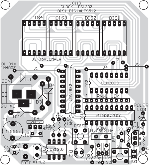
Fig. 1 shows the circuit of the microcontroller based clock. It comprises microcontroller AT89C2051 (IC1), inverting buffer ULN2003 (IC2), real-time clock (RTC) DS1307 (IC3), regulator 7805 (IC4), non-inverting source driver UDN2982 (IC5) and a few discrete components.
Microcontoller AT89C2051 is the heart of the clock. It is an 8-bit microcontroller with 2kB Flash programmable and erasable read-only memory (PEROM), 128 bytes of RAM, 15 input/output (I/O) lines, two 16-bit timers/counters, a five-vector two-level interrupt architecture, a full-duplex serial port, a precision analogue comparator, on-chip oscillator and clock circuitry.

Port pins P1.7 down through P1.1 of the microcontroller are pulled up with 10kΩ resistor network RNW1 and connected to input pins 1 through 7 of inverting buffer IC2, respectively, to provide segment data for the seven-segment display. The display shows the time as ‘hour.minute.’ Flashing of decimal point (dp) on DIS3 indicates the seconds. The decimal points for DIS1 and DIS2 are not used here.
The selection of the four seven-segment displays is made by port pins P3.7, P3.4, P3.5 and P1.0 of the microcontroller. These pins drive the four non-inverting buffers of driver IC5 to provide display-enable signal to the common-anode pin (either pin 3 or pin 8) of DIS1 through DIS4, respectively. If UDN2982 is directly given an unregulated 9V supply, it can support even bigger-size seven-segment displays (refer Fig. 1). The microcontroller provides the segment data and display-enable signal simultaneously in time-division-multiplexed mode for displaying a particular number on the seven-segment display. Segment data and display-enable signal for display are refreshed every four milliseconds, so the display appears to be continuous.
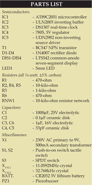
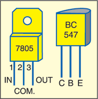
Switch S1 is used to reset the microcontroller manually, while the power-on reset signal for the microcontroller is derived from the combination of capacitor C3 and resistor R2. A 11.0592MHz crystal is used to generate clock frequency for the microcontroller. When the alarm time is reached, port pin P3.3 provides aural indication signal to the base of transistor T1. Transistor T1 conducts and the piezobuzzer sounds for one minute.
Timing inputs are generated by RTC DS1307. It is a low-power, real-time, full binary-coded decimal clock/calendar having 56 bytes of non-volatile static random-access memory (RAM). Address and data are transferred serially via a two-wire, bi-directional bus. The clock/calendar provides seconds, minutes, hours, day, date, month and year information. Battery connection at pin 3 provides battery backup. The battery (CR2032) works for two to three years.
The display and alarm are controlled by microcontroller AT89C2051. Data is transferred between microcontroller AT89C2051 and the RTC using two wires (which form the I2C bus), one of which serves as the clock line (SCL) and the other as data line (SDA). The four subroutines required for data transfer are the send-start condition, send-stop condition, read-a-byte and write-a-byte. Using these subroutines, the time of the day can be written into internal registers of the RTC at address locations 00H through 06H (refer the datasheet). The address of the control register is 07H. If it is written with control word 10, a 1Hz square wave is available from pin 7 of the RTC. The pulse output at pin 7 drives pin 5 (dp) of DIS3, which blinks every second.
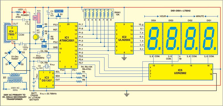
The RTC is driven by an external 32.768kHz crystal. A 3V battery is connected at its pin 3 along with 1μF capacitor for battery backup. Pins 5 and 6 are pulled up to 5V by resistors R5 and R4 and connected to pins P3.1 and 3.0 of the microcontroller, respectively, for serial communication between the RTC and the microcontroller.
To derive the supply power for the circuit, the 230V, 50Hz AC mains is stepped down by transformer X1 to deliver a secondary output of 9V, 500mA. The transformer’s output is rectified by a full-wave bridge rectifier comprising diodes D1 through D4, filtered by capacitor C1 and regulated by IC 7805 (IC4). Capacitor C2 bypasses the ripples present in the regulated output. LED1 acts as the power indicator. Resistor R1 acts as the current-limiter for LED1.
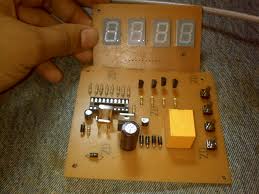
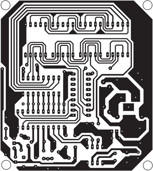
An actual-size, single-side PCB for the microcontroller-based clock using DS1307 is shown in Fig. 3 and its component layout in Fig. 4.
Setting of current time and alarm time
To set the alarm time, press switch S2 connected to pin P3.2 of the microcontroller and keep it pressed until the display changes and reaches the required alarm time, say, 7:30. Now connect the pole of SPDT switch S3 to Vcc momentarily (which makes pin P3.3 of the microcontroller high) and bring it back to the initial position. Immediately, the alarm sounds for a minute. The alarm time is thus set at 7:30.
To set the current time, keep switch S2 pressed until the time display reaches the current time. Release it when the current time is set.
Once the time is set and the clock is working, there is no need to set the time again even after switching off the circuit. This is because the RTC works off the 3V battery connected to its pin 3.
Download PCB and component layout PDFs: click here
Software
The source code is written in Assembly language and assembled using a cross-assembler (ASM51). It is well-commented and easy to understand.
The program uses internal Timer0 of the microcontroller for periodic data output to the LED displays. Timer0 is programmed as a 16-bit timer. The timer starts from F0FFH and overflows at FFFFH. On every overflow, its interrupt function is enabled. The interrupt service routine refreshes the display. For this, the minutes and hours data is read from the RTC and displayed on the seven-segment display.
For setting the time when switch S2 is pressed, the time is incremented and stored into the RTC. Set the alarm time by using switch S2 in combination with switch S3. The set time is stored in the RTC in two RAM locations. Every time the clock-time changes, it is compared with the stored alarm time value and if both are same, pin 7 of the microcontroller becomes high. Transistor T1 conducts and piezobuzzer PZ1 sounds for a duration of one minute.
Download source code: click here
You may also like other circuit projects
The project was originally published in September 2012 and has been recently updated.
Can u please upload tha c file?
When I connect no.1 pin and no.20 pin of 2051, the display is off. What’s tha problem?
me gustaria conseguir este para 12 horas pues esta a 24 horas donde lo consigo ?
Ic ki programing send kro sir plz..
This clock 12 hrs.or24 hrs mode?
Hi
I want to have separate button to set minute and hour
help me
Thankful