


 Pulse-width modulation (PWM) is one of the oldest and widely used techniques of controlling electrical motors. To control the speed of the motor, the average value of the PWM pulse is controlled by a switch. If the switch is ‘on’ for a long duration, the average value of the PWM pulse increases, driving the motor to high speed, and vice versa. The advantage of using PWM is that there is minimal power loss in switching devices.
Circuit Description for Motor Speed Control
Most circuits use a potentiometer as the variable switch to generate PWM. It is cumbersome to use because it needs manual movement of the potentiometer by the user. In this circuit, we use thermometer decoding circuit to control the switch resistance. This, in turn, controls the duty cycle of the pulse, thereby producing PWM. In order to verify the proposed circuit, we have used a circuit simulation software called LTspice.
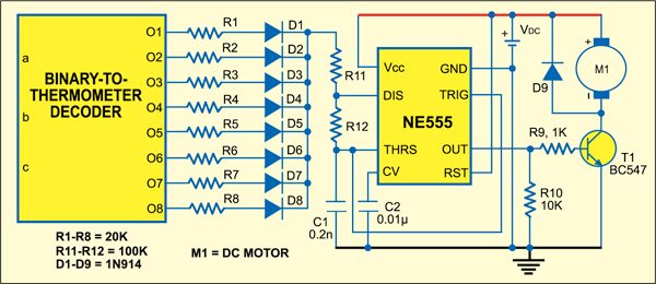

The circuit mainly consists of the following components: 3-bit counter, binary-to-thermometer decoder logic, 555 timer IC, resistors (R1-R8=20 kilo-ohms, R11=R12=100 kilo-ohms), diodes (1N914), capacitors (C1= 0.2 nF, C2=0.01 µF) and supply voltage (VDC= 5V).
The complete circuit is shown in Fig. 1 produces the PWM pulse for motor speed control. Fig. 2 shows the internal diagram of the binary-to-thermometer decoder with binary inputs coming from the 3-bit ripple counter.

Counter
We have used the 3-bit ripple counter to count all the eight possible states. Clocking to counters is given by clock 1, which is controlled by reset (RST) signal through the AND gate as shown in Fig. 2. This is done so that the RST pulse allows you to see a particular digital state. Otherwise, you will see all the eight possible states of the counter.
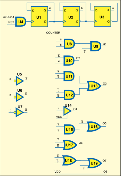
Note that signal wires from the counter are fed to various input points of the binary-to-thermometer decoder logic through inverters U5, U6 and U7.
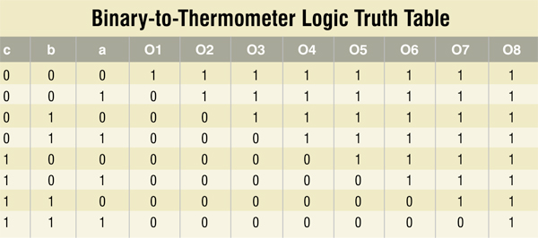
Binary-to-thermometer logic
Refer the binary-to-thermometer truth table for 3-bit binary inputs.
Here a, b and c are the inputs coming from the 3-bit counter, while O1 through O8 are the outputs of the thermometer decoder which are connected to 555 timers through the array of 20-kilo-ohm resistors and 1N914 diodes. Timer IC 555 is running in astable mode.
Charging time is given by:
Tc = 0.69C1(R11+R12+RTUNE)
Discharging time is given by:
Td = 0.69C1R12
RTUNE is the effective parallel resistance of R1 through R8 depending on the digital code. Tc varies as the digital code (a,b,c) changes, and so does the duty cycle. This is because, as we can see from the truth table, the number of 1’s coming out of the decoder logic depends on the binary code.
For example, binary code 001 applied to decoder logic results in making O1 ‘off’ and the rest of the outputs (O2 through O8) ‘on’. In this case, all the diodes connected to O2 through O8 are forward-biased and hence all the resistors (R2 through R8) connected to these ports come in parallel with each other to give RTUNE, thereby changing the charging time (TC) of the 555 timer circuit. However, the diode connected to O1 is ‘off’ as it is reverse-biased and hence its resistor R1 doesn’t add to RTUNE.
For binary input 111, only one resistor, i.e., R8, is connected to the 555 timer, thereby producing a pulse with of a smaller duty cycle than with binary input 000.
Consequently, 555 timer produces a pulse-width-modulated signal with varying pulse width at its OUT port which can drive the motor with variable speed as the average value of PWM pulses varies. Speed is fast when the binary input is 000 and very low when the binary input is 111. The timer output from OUT port is then fed to transistor T1, which acts as a driver circuit for motor control.
SPICE Software
We have used LT-Spice IV simulation software to test the circuit. You can download the simulator free of cost.
After download, open the application, click ‘File’ menu and draw new schematic diagrams as given here and name the file as Motor_control.asc. In this project, along with this .asc file, there are two other files: DFF.asc and sample_and_ hold.asc. These files contain the D-type flip-flop and sample-and-hold circuits that are part of the design, so they need to be defined in the software. Basically, these two files are used in designing the counter.
Use Motor_control.asc file for simulation. To see the simulation output, follow the steps given below:
1. Click ‘Simulate’ button from the menu bar followed by ‘Run’ button. The Motor_control.raw simulation window appears.
2. Select ‘Plot Settings’ option.
3. Select ‘Add Trace’ option. A box will appear.
4. Select ‘v(pwm_out)’ option to get the output.
Source code: click here
Simulation results
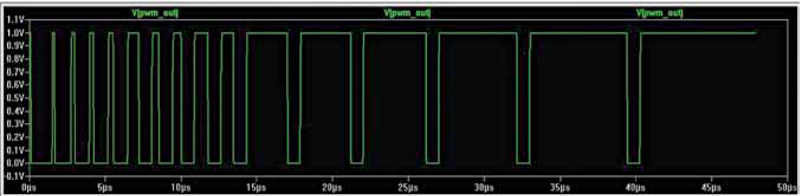
Fig. 3 shows the simulation result of the schematic shown in Fig. 1 without RST logic but with clock signal given directly to the counter. You can also click OUT pin of 555 timer circuit to see the pulse-width-modulated output. Here you can see that the duty cycle of the waveform continuously changes as the binary code transitions from 000 to 111. If these pulses are fed to a DC motor, the speed of the motor will vary as per the width of the pulse train.

Where is the thermal effect here , hence the word Thermometer ?