


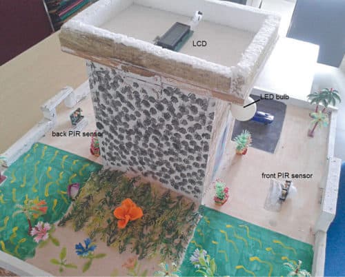
 This project demonstrates a wireless security system in which four pyroelectric infrared (PIR) motion sensors are placed in four sides—front, back, left and right—of the area to be covered. It detects motion from any side and turns on the audio-visual alarm. It also displays the side where the motion (intruder) is detected. All sensors send signal to the central controller circuit wirelessly. The author’s prototype arrangement is shown in Fig. 1.
System block diagram
System block diagram of the wireless security system is shown in Fig. 2. The project uses PIR motion sensors to detect motion and ASK-based radio frequency (RF) transmitter and receiver modules to send signals wirelessly. It uses AT89S52 microcontroller (MCU) and LCD to display the side where the motion is detected.
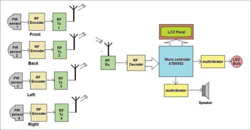
The block diagram has two parts: four transmitter units with PIR sensors, encoders and RF transmitters; and receiver unit with RF receiver, decoder, MCU and some audio-visual circuits.

Transmitter unit
There are four transmitter blocks, one each for front, back, left and right sides. Each block consists of a PIR sensor, RF encoder chip and RF transmitter (Tx) module.
PIR sensor
The PIR sensor detects motion by measuring any change in IR levels emitted by objects. Pyroelectric devices have elements made of a crystalline material, which generate an electric current when exposed to IR radiation. Changes in the amount of IR falling on such devices changes the voltages that are generated. Sensor output goes high when it detects motion. Sensor output is given to RF encoder chip.

RF Encoder
HT12E encoder chip encodes PIR sensor output into serial bit streams and gives it to RF Tx module.
RF transmitter
ASK transmitter modulates incoming digital signals from the RF encoder using a 434MHz carrier and transmits it through its antenna.
Receiver unit
This is the central controlling section that receives signals from any of the four PIR sensors at the transmitter side. It gives audio and visual alarms, and displays the side where the motion is detected on LCD1.
RF receiver
This module operates on 434MHz frequency and demodulates the received digital signals before sending bit streams to RF decoder chip.
RF decoder
HT12D RF decoder chip decodes bit streams and generates parallel 4-bit digital output, which is given to the MCU.
MCU
AT89S52 MCU performs the following tasks:
1. Detects side where motion is detected from RF decoder digital output
2. Displays various messages including side of detected motion on LCD1
3. Turns on speaker and blinks LED for audio-visual alarm when motion is detected
LCD panel
The 16×2 LCD panel displays messages given by the MCU.
Multivibrators
There are two multivibrators. One for blinking the LED at low frequency (1Hz – 2Hz), and the other for generating the audio frequency signal (1kHz) through the speaker for siren.
Circuit and working
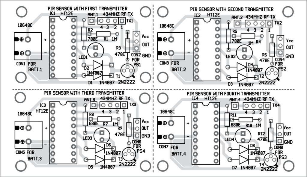
There are five circuits. Of these, four transmitter circuits are similar to each other, with minor changes, as shown in Fig. 3. Fifth circuit, as shown in Fig. 4, is the receiver circuit.
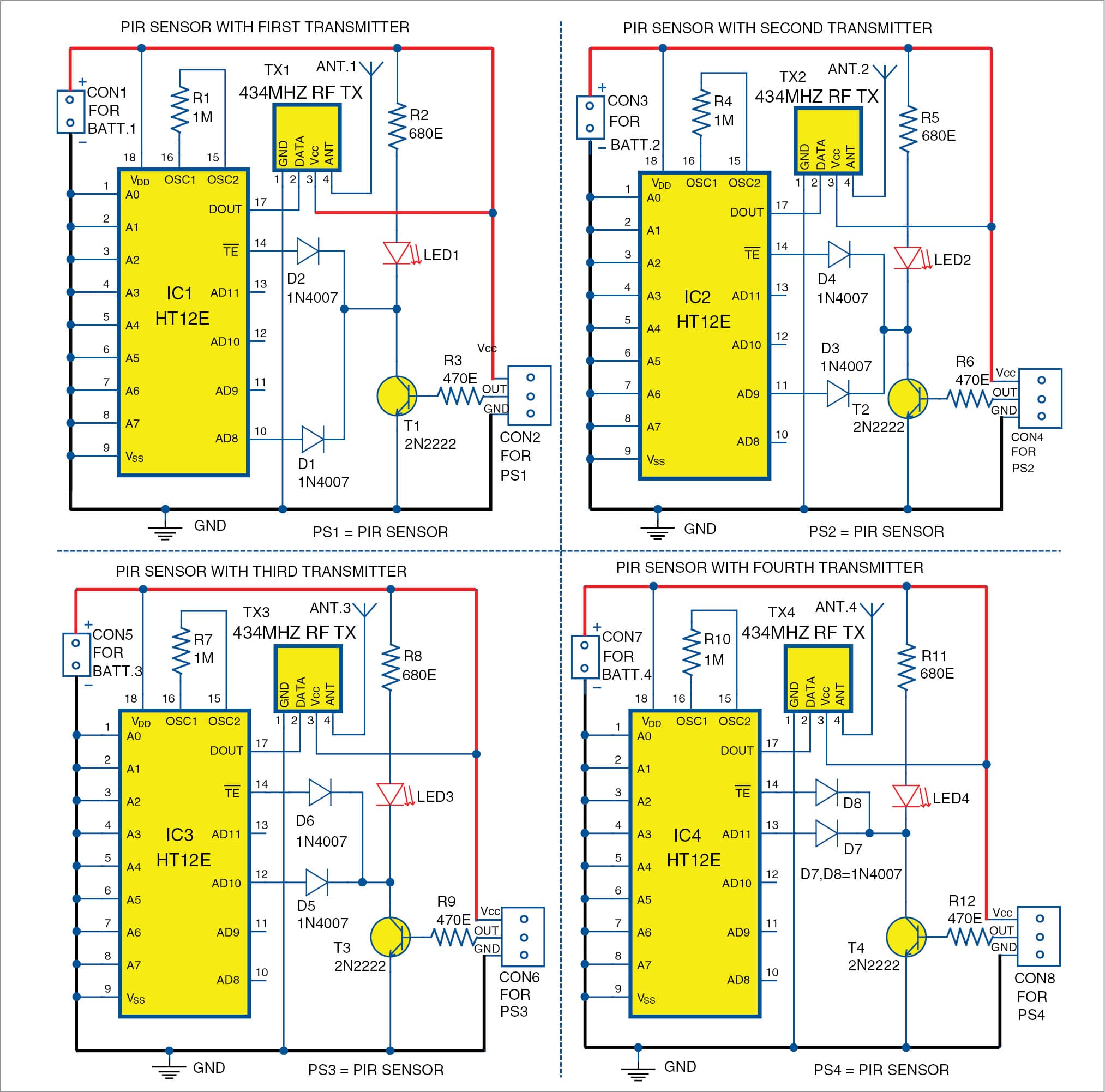
Transmitter circuit
The first transmitter circuit is built around IC1. Output of PIR sensor PS1 is given to data input AD8 (pin 10) of HT12E (IC1) after inverting it through transistor T1. Diodes D1 and D2 connect transmission enable (TE) pin with pin AD8, so that both pins get input from the sensor at the same time.
LED1 is connected to collector output of T1, so that it blinks when PS1 sensor output goes high. Address pins A0 through A7 of IC1 are connected to ground to set address 00 (0000 0000b). Serial data output DOUT (pin 17) is given as data input to 434MHz RF Tx module (TX1). The whole circuit is given power through 6V battery (BATT.1) connected across CON1.
The other three circuits are shown in Fig. 3 are similar to the one described above. The only difference is that the diode is connected to different data pins.
When PIR sensor PS1 detects motion, its output goes high. T1 conducts and LED1 blinks.
Pins AD8 and TE of IC1 are pulled low together through diodes D1 and D2. When TE pin is pulled low, IC1 transmits address A0 through A7, and AD8 through AD11 serially through RF Tx module. Because pin AD8 is pulled low, data bits are transmitted as 1110 (AD11 through AD8). Similarly, in other such circuits, when motion is detected, the respective data pin is pulled low, so different data is transmitted, as listed in Table I.
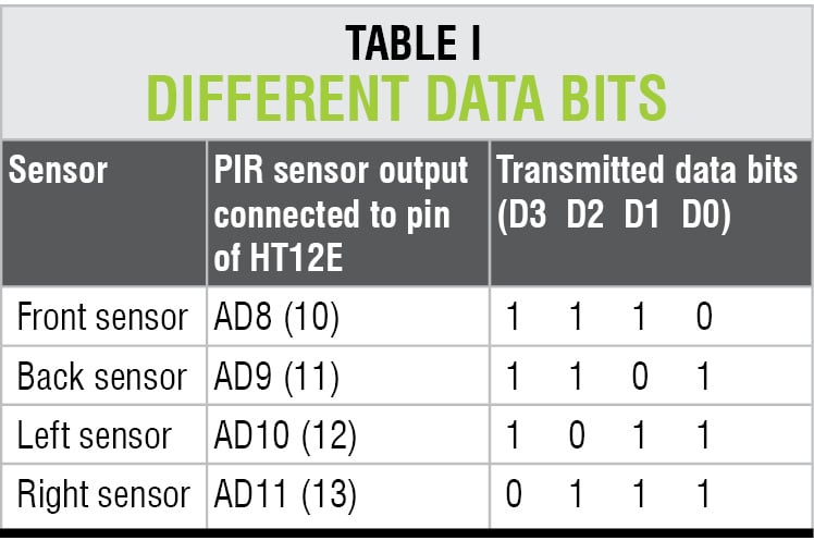
Thus, when a sensor detects motion from its side, different bit pattern of D0 through D3 is transmitted. At receiver side, this pattern is used to identify the side where motion is detected.
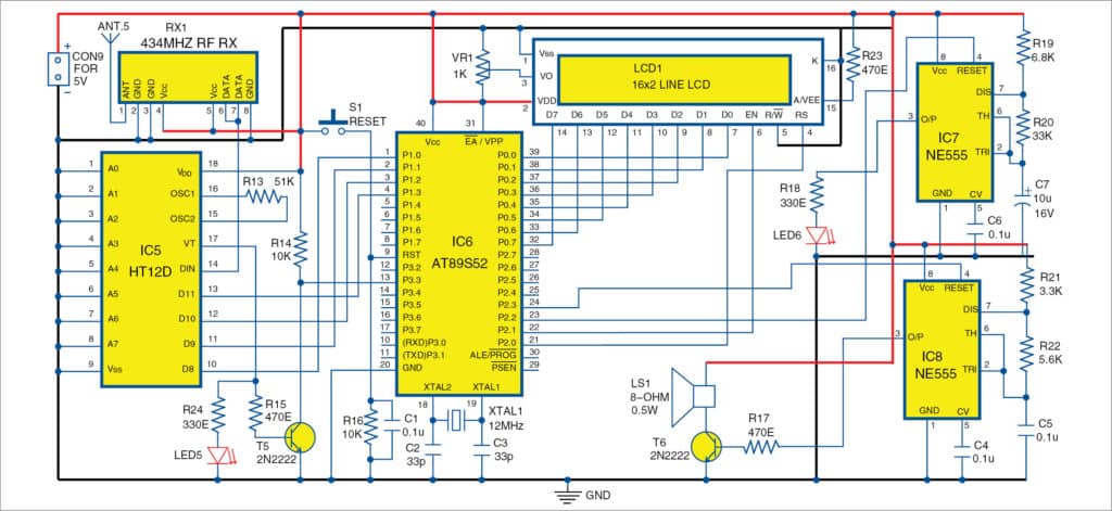
Receiver unit
As shown in Fig. 4, the receiver is built using 434MHz RF Rx module (RX1), RF decoder chip HT12D (IC5), AT89S52 MCU (IC6) and NE555 multivibrators (IC7 and IC8).
Serial data output from 434 RF Rx module is given to data input pin 14 of HT12D decoder.
Address pins A0 through A7 of HT12D are connected to ground to set same address 00 (0000 0000b) as encoder. LED5 is connected to VT (valid transmission) pin, which blinks to indicate that data is received. The same VT output is inverted using T5 and given to external interrupt pin EX1 (pin 13) of AT89S52. Data output pins D8 through D11 are connected to port pins P1.0 through P1.3, respectively.
LCD1 data pins D0 through D7 are connected to port P0 of IC6. Control pins RS and EN are connected to port pins P2.0 and P2.1 of IC6, respectively. Pin R/W is connected to ground to enable LCD1 write. Preset VR1 is connected to pin 3 to vary LCD1 brightness. Backlight LED pins 15 and 16 are connected to +5V via R23 and ground, respectively, to turn on LCD1 backlight.
There are two multivibrator circuits. Both are built using IC NE555 and configured in astable mode. Reset pin 4 of both multi-vibrators are controlled by MCU port pins P2.2 and P2.3.
A 12MHz crystal is connected to crystal pins 18 and 19 of IC6 along with two 33pF capacitors (C2 and C3). This circuitry provides clock signal to the MCU for its internal operations. Capacitor C1 in parallel with resistor R16 and push button S1 are connected to RST pin 9 to provide manual reset to the MCU.
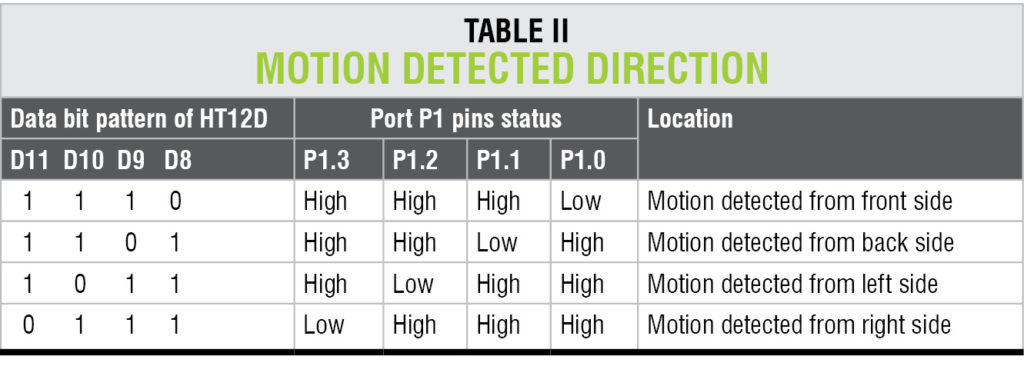
When any sensor detects motion, data is transmitted through RF Tx. This is received and demodulated by RF Rx module. This data is sent to RF decoder HT12D (IC5), which detects valid address indicated through the blinking of LED5. Then, the decoder latches the data, which is made available across data pins D8 through D11 of IC5. When valid address is received, VT pin of IC5 goes high and the MCU gets an interrupt signal. It gets bit pattern on port P1. As per data bits, any one pin (out of four) will be low and rest will be high.
Based on which pin is low, the MCU identifies the sensor that detects motion and indicates the direction of the intrusion. This is listed in Table II.
As per Table II, the MCU immediately decides and displays the message “intruder detected from xxxx side” on LCD1. It also enables both multivibrators by applying high input on RST pin.
The multivibrator (IC7) that flashes LED6 has a flashing rate of 2Hz. Component values for R19, R20 and C7 are chosen in a way that output frequency is around 2Hz.
Another multivibrator (IC8) generates 1kHz audio tone as siren through speaker (LS1). Component values for R21, R22 and C5 are chosen in a way that output frequency is around 1kHz.
When sensor PS1 (or any sensor) detects motion, its output remains high for around five to ten seconds because of a slower response. The siren sounds and LED6 continues flashing for about ten seconds. The message on LCD1 shows the side where motion is detected.
After sensor output becomes stable (low), both the siren and LED6 turn off.
Software program for Wireless Security System
Complete system operation is carried out based on the program embedded into the internal flash of AT89S52. The program performs the following tasks:
1. Decides where motion is detected
2. Displays warning and other messages on LCD1
3. Displays side where motion is detected
4. Flashes LED6 and turns on siren when motion is detected
The program is written in C language for 8051 family of controllers. It is compiled in Keil IDE software. The complete program is a combination of many different functions, including:
lcd_delay() generates delay for the LCD to get ready to accept a new command or data byte
lcd_send_cmd() sends command byte to LCD
lcd_send_data() sends character to be displayed on LCD
lcd_display_string() displays various strings and messages on LCD
lcd_init() configures and initialises LCD
ext_int() is an interrupt sub-routine function that gets input from port P1
delay_10s() generates approximately 10-sec delay
main() compares digital input of P1 and detects which port pin is low. It also displays on LCD1 the side of motion or intrusion detection
Download Source Folder
Construction and testing
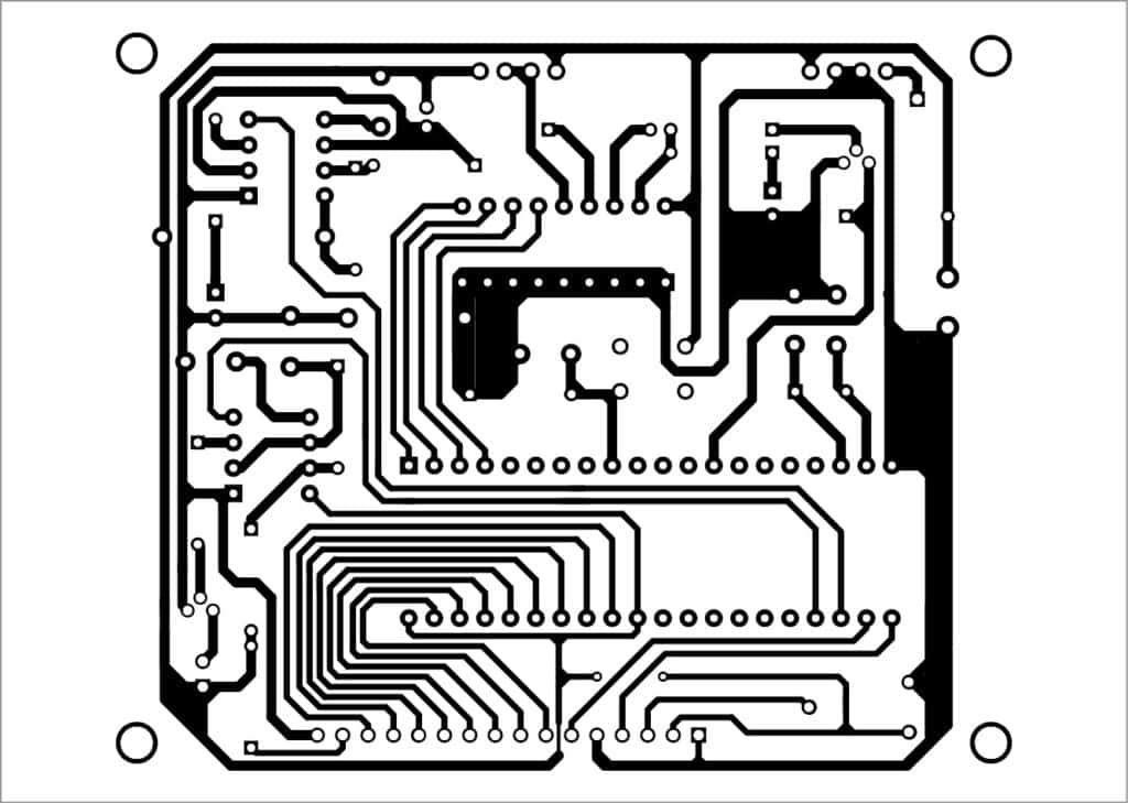
An actual-size PCB layout for the transmitter section of the wireless security system is shown in Fig. 5 and its components layout in Fig. 6.
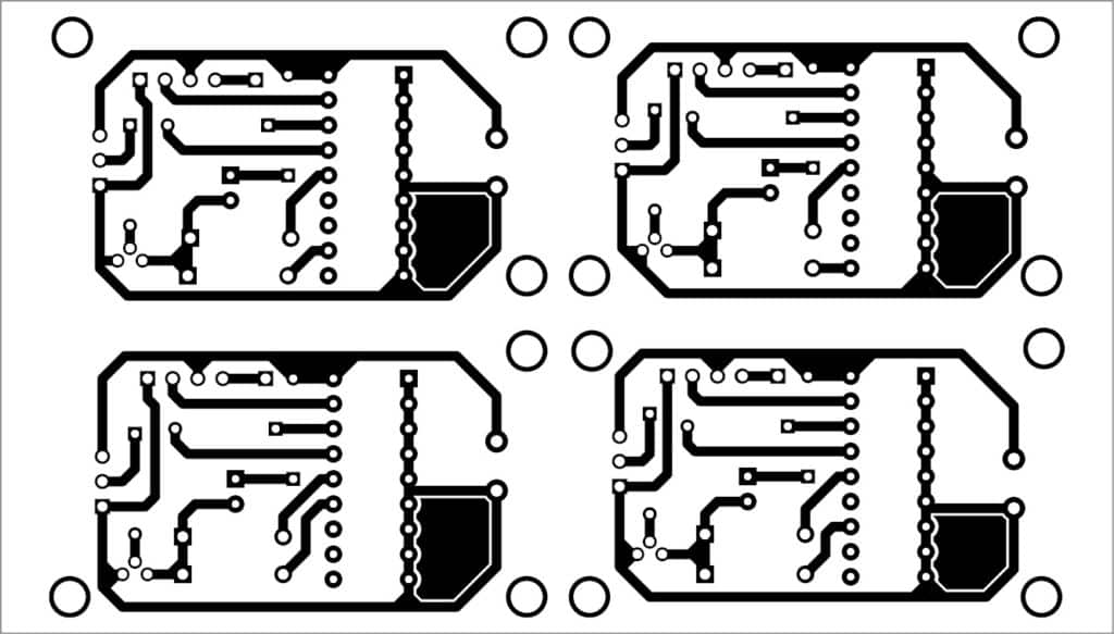
Cut the PCB across the dotted lines for four transmitter sets. Enclose each transmitter section in separate boxes, including 6V battery. Connect the four PIR sensors in each transmitter PCB assembly. Install these at the four locations of your home or office.
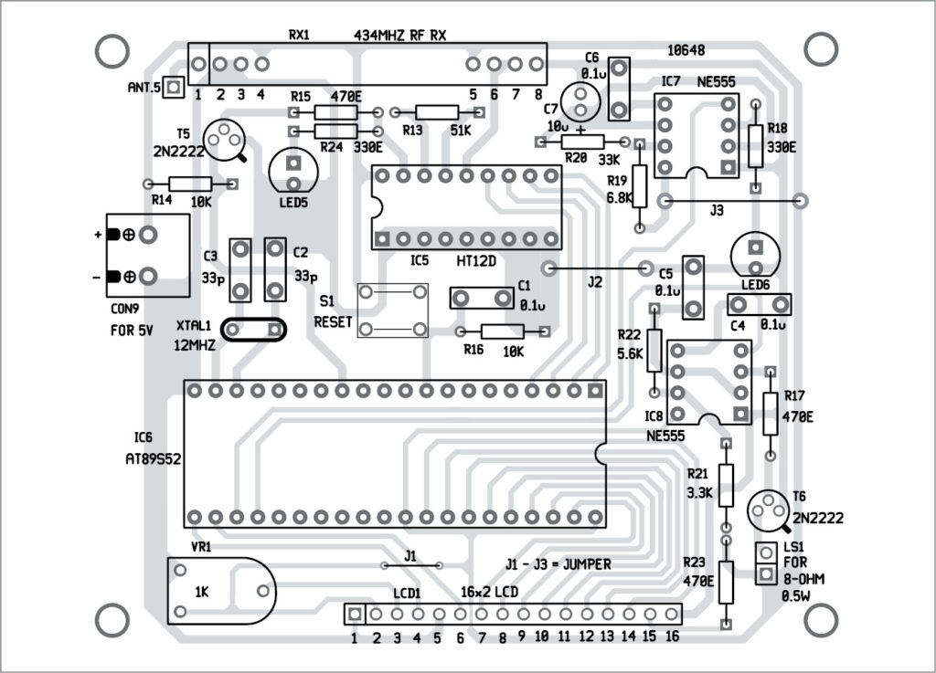
An actual-size PCB layout of the receiver unit is shown in Fig. 7 and its components layout in Fig. 8.
Download PCB and component layout PDFs: click here
After assembling the circuits on the PCBs, if everything is correct, burn the program (pir.hex) into the MCU using a suitable programmer. Insert AT89S52 on IC base soldered on the PCB. Enclose the PCB, switch and connectors in a suitable box. Connect 5V to operate the circuit. Your circuit is now ready to use.

I would like to build such a system,,, and many thanks for your clear description of the process,,, I hope I am able to build it. Cheers and thanks.
Thank you for your feedback.
sir, in wireless security using pir sensor is prorgm based or only for hard ware implrmentation.
Sir ,I used 89c51 ic is it able to run project?
Sir, I’ve tried to make this project but the problem is in transmission and reception. Can u tell me which transmitter and receiver module uve used?
can i use 433Mhz transmitter for this?
What compiler did you use and how did you program the AT89Ð
Diodes D1 and D2, are they not supposed to be the other way to let signal pass through them to the MCU?
are D1 and D2 or one of them supposed to be in the other direction to let signal in to MCU?
//I am asking it for second time because the previous comment is not visible on my side//
This is not working, I tried it
Kindly elaborate your query.
I tried it, but not working. really useless
Kindly elaborate your query.
I tried it using a 433Mhz transmitter-receiver pair and a raspberry pi at the central receiver circuit instead of a microcontroller. and it worked perfectly.
Dear Charles,
Thanks for interfacing this circuit with raspberry pi.
Regards
Sir, instead of 1N4007 rectifier diode, can I use 1N4148 or 1N914 for D1-D8?
Dear Sir,
Yes. You can use 1N4148 instead of 1N4007 rectifier diodes.
Regards