
Can compact isolation structures enable denser 5G antennas? PCB-friendly isolation techniques make it possible to place more antennas into tight layouts without sacrificing isolation, gain, or efficiency.
Designers of 5G radios face a constant squeeze: product teams demand more antennas in less space to support higher capacity, beamforming, and MIMO, while RF physics penalises elements placed too close together. As spacing shrinks, mutual coupling quietly degrades matching, distorts radiation patterns, and reduces array efficiency.

Across antenna research and consulting projects for 3.5GHz 5G systems, the outcome often depends on how effectively coupling is controlled within just a few millimetres of PCB space. Small layout decisions in this narrow gap frequently determine whether an array performs reliably or falls short.
Compact isolation structures, such as parallel-coupled line resonators and carefully shaped ground features, provide a practical way to increase antenna density in 5G and future systems. These solutions fill the limited gaps already available, use standard PCB processes, and deliver measurable isolation improvements in real hardware.
Why spacing alone is not enough
The simplest way to reduce coupling is to increase the distance between elements. For many 5G arrays at 3.5GHz, designers aim for element spacings around half a wavelength. That approach works until mechanical constraints, size limitations, and multi-band packaging push antennas closer together.
Once you move below these comfortable spacings, following happens:
- Surface waves on the substrate become a significant coupling path.
- The input impedance of each element changes due to its neighbours.
- Radiation patterns and front-to-back ratio degrade, directly impacting coverage and MIMO performance.
In consulting work, I have seen arrays that simulated well as isolated elements but failed in the final product because real-world spacing and housing forced much tighter layouts. At that point, we can no longer ‘buy’ isolation with space; we must engineer the coupling path itself.
There are many published solutions: defected ground structures (DGS), electromagnetic bandgap (EBG) patterns, complementary split-ring resonators, metamaterial-inspired structures, and even vertical isolation walls. These approaches work, but they often require extra board area, non-planar structures, or complex geometries that may not be suitable for cost-sensitive, high-volume hardware.
Compact isolation: think in the gap, not around it
A common mistake is to look for large or exotic solutions—extensive EBG lattices, tall 3D structures, or bulky chokes, when only a few millimetres of real estate are available. In practice, compact isolation structures placed directly in that gap are easier to deploy and integrate.
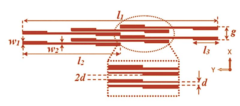
In our 3.5GHz mutual-coupling work, the parallel coupled-line resonator (PCR) fits entirely between two closely spaced patches on FR-4. The element functions as a local band-stop filter at the operating frequency, so currents attempting to flow between patches encounter high impedance in that narrow region.
Key lessons from deploying and testing these kinds of structures:
- Treat the gap between antennas as a functional area, not a wasted board edge
- Design isolation elements that share the same planar technology and stackup as the antennas
- Aim for resonant or slow-wave behaviour within your band of interest, rather than broad, heavy structures
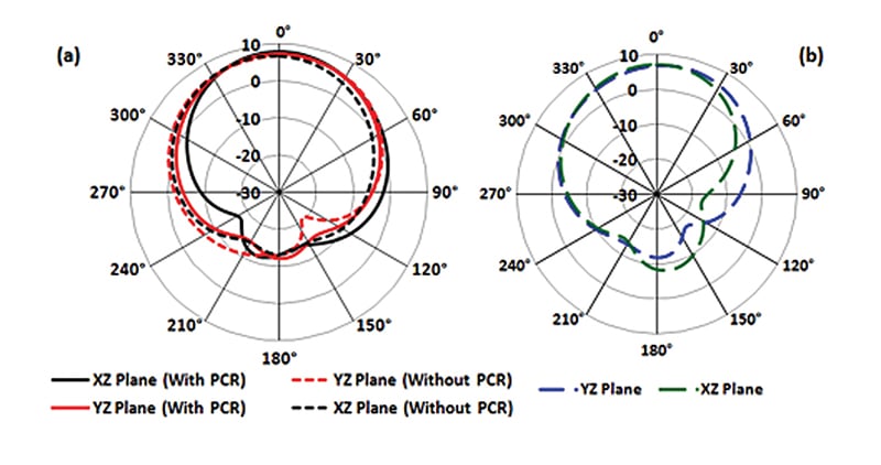
Case study: PCR-based isolation in a compact 3.5GHz array