





A technique to control where atomically thin semiconductor crystals begin growing, potentially enabling high-quality stacked chips that reduce data-transfer delays and energy consumption in future AI hardware.
Researchers from the Korea Advanced Institute of Science and Technology (KAIST), in collaboration with other institutions, have developed a technique that precisely controls where two-dimensional (2D) semiconductor crystals begin forming. The method could help overcome a manufacturing challenge in stacking semiconductor devices vertically to improve AI chip performance and energy efficiency.
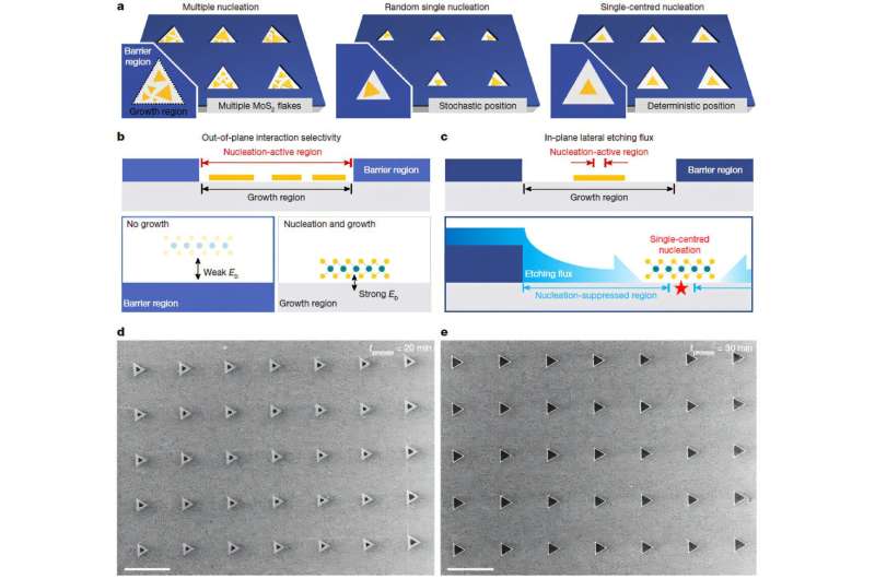
The technique, called etching-flux-mediated single-centered nucleation (EF-SCN), enables a semiconductor crystal to begin growing at a predetermined location rather than at multiple random points. In experiments, researchers achieved single-crystal growth at the designated centre in more than 99% of 400 tested patterns.
The development addresses a key limitation in manufacturing atomically thin semiconductor layers directly on existing electronic circuits. Two-dimensional semiconductors, such as molybdenum disulfide (MoS₂), are only a few atomic layers thick and can retain useful semiconductor properties at extremely small dimensions. Their thin structure makes them promising candidates for vertically stacked electronic devices, in which computing and memory circuits are placed closer together.
Such architectures can shorten the distance data travels between processing and storage units, potentially reducing latency and energy consumption. However, manufacturing these structures requires semiconductor films to grow precisely where they are needed. During conventional crystal growth, nuclei the initial formations from which crystals develop can appear at several locations. As these crystals expand and meet, they form grain boundaries that can impede electron movement and reduce material quality.
EF-SCN addresses this problem by using oxygen released from an oxide barrier, such as hafnium oxide (HfO₂). The oxygen acts as an etching flux, suppressing the formation of new crystal nuclei near the barrier. This effect weakens towards the centre of the designated growth region, allowing a single crystal to form there and expand while competing nuclei are suppressed. The researchers also demonstrated the method’s compatibility with more complex material structures. They grew lateral heterostructures combining MoS₂ and molybdenum diselenide (MoSe₂), then selectively deposited a thin ruthenium metal film on the MoSe₂ regions.
The results suggest that controlling nucleation could support the direct fabrication of high-quality semiconductor layers on existing chips, reducing reliance on growing materials separately and transferring them onto circuits. If adapted for manufacturing, the technique could help enable stacked-channel architectures for future AI processors and other high-performance electronic systems. However, further development is needed to establish its suitability for large-scale chip production.
