


AI and data center chips are hitting limits. A new 3D chip design improves speed, power use and memory bandwidth.
Data center, AI, and HPC designers face growing limits in performance, power efficiency, and memory bandwidth as AI models become more complex. Traditional planar chips struggle because communication between dies is confined to the edges, creating bottlenecks in speed and functionality. Moore’s Law alone can no longer meet the demands of next-generation computing.
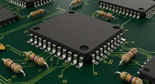
Alphawave Semi has successfully completed the tape-out of its UCIe 3D IP on TSMC’s advanced SoIC technology within the 3DFabric platform. This milestone builds on Alphawave Semi’s existing UCIe IP portfolio and marks a major step forward in its chiplet integration capabilities. Using TSMC’s SoIC-X 3D packaging, the company enhances power efficiency, performance, and bandwidth for next-generation datacenter, AI, and HPC applications.
The IP supports face-to-face (F2F) configurations, offering a 10x improvement in power efficiency compared to traditional 2.5D die-to-die interfaces and up to 5x higher signal density.
As AI models become more complex, traditional scaling approaches like Moore’s Law cannot keep up with growing demands for performance, power efficiency, and memory bandwidth. In planar designs, chip-to-chip communication is limited to the perimeter, restricting bandwidth and functionality within a package.
To overcome these limits, designers are moving beyond monolithic SoCs to disaggregated architectures, rethinking how memory, I/O, and logic are combined. Advanced packaging, including horizontal expansion or vertical die stacking, offers a path forward. 3D die stacking in particular improves bandwidth density and power efficiency.
Alphawave Semi’s UCIe-3D solution features a 5nm bottom die with TSVs that supply power and ground to a 3nm top die. Its 3DIO portfolio also includes a proprietary design flow and methodology for fast, efficient 3D stack construction and verification.
“This successful tape-out represents a significant milestone for Alphawave Semi and our AI platform,” said Mohit Gupta, Executive Vice President & General Manager, Alphawave Semi.”By combining our high-speed 3D UCIe IP with TSMC’s groundbreaking SoIC-X technology, we are directly addressing the memory and bandwidth bottlenecks that limit our customers’ next-generation AI and HPC applications. This is a testament to our team’s innovation and our commitment to enabling a new class of chiplet-based systems.”
