


Researchers have developed a physics-based technique that accurately measures atomic-scale semiconductor defects, helping improve power electronics used in electric vehicles, renewable energy systems, and next-generation high-efficiency devices.
Researchers from Auburn University and Sandia National Laboratories have developed a new semiconductor measurement method that could significantly improve the reliability and efficiency of future power electronics. The breakthrough addresses a decades-old challenge in accurately identifying atomic-scale defects at the interface between semiconductors and insulating materials.

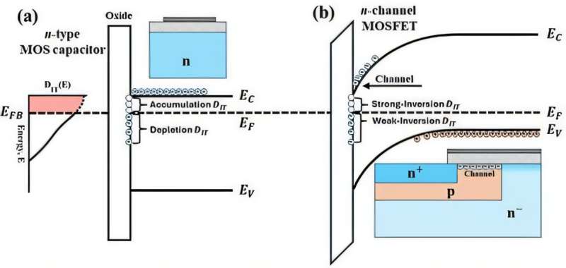
These microscopic defects, though often invisible during normal device operation, can trap electrical charges and degrade the performance of high-power semiconductor devices over time. Such failures are especially critical in technologies like electric vehicles, renewable energy converters, and advanced industrial electronics, where efficiency and reliability are essential.
Conventional defect-analysis techniques rely on comparing device responses to fast and slow electrical signals. However, the accuracy of these measurements depends heavily on estimating insulator capacitance with extreme precision. Even minor inaccuracies can produce misleading defect readings, limiting engineers’ ability to properly evaluate semiconductor interfaces.
The newly proposed framework removes this uncertainty by applying a physics-based electrostatic consistency check. Instead of relying on estimated parameters, the method automatically identifies correct operating conditions by ensuring voltage relationships inside the device obey fundamental physical laws. This allows researchers to obtain more reliable defect measurements, particularly near semiconductor band edges where performance-impacting defects are most active.
According to the research team, the technique is especially important for wide-bandgap semiconductor materials such as silicon carbide and gallium nitride. These materials are widely used in high-efficiency power electronics but are highly sensitive to interface defects that can reduce switching performance and increase power losses.
The study, published in the Journal of Applied Physics, is expected to help semiconductor researchers better understand material behavior and optimize next-generation electronic devices. Improved defect characterization could ultimately support the development of faster, more energy-efficient, and longer-lasting electronics for automotive, energy, aerospace, and industrial applications.
