
Copper nanowires connections can be made at room temperature with limited bonding pressure, suitable for thin, heat-sensitive chips.
The research team at Fraunhofer IZM-ASSID, in collaboration with industry and academic partners, has made a significant breakthrough in connection technology for electronic chips, using nanowires at a nanometer scale. Successfully demonstrated for industrial production on 300 mm silicon wafers, the researchers explored copper nanowires as a promising alternative for contacts shrunk to less than 10 mm.

Traditional flip-chip designs using copper bumps for soldering are reaching their physical limits, especially as devices shrink further. Issues like solder leakage can cause short circuits in the system. This approach offers several advantages over traditional methods like copper soldering or solder bumps, including the ability to create designs with different heights, mechanical robustness, and freedom in chip design.
The team focused on developing new interconnection technologies to meet the increasing demand for smaller pitches (the space between electronic contacts) on chips. This allows for more transistors and electronic circuits on a chip, enhancing its power and efficiency.
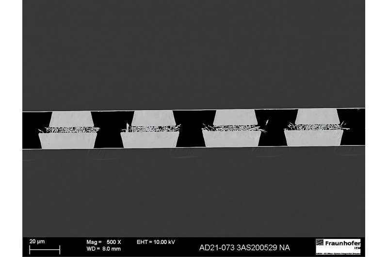
A critical aspect of the project was ensuring the even growth of nanowires across the entire 300 mm wafer. This was achieved using special membranes with tiny pores to determine the nanowire thickness, varying from 100 nm to 1 µm.
The connections using copper nanowires can be made at room temperature and with limited bonding pressure. This makes the technology resource-efficient and suitable for thin or heat-sensitive chips.
The project culminated in the production of a 300 mm silicon wafer with homogeneous nanowire bumps and connections, showcasing the integration potential in 2.5D to 3D system designs. Plans are underway to further shrink the contacts to 10 or even 5 micrometres, with potential applications for complex packages requiring fine-pitch or larger contact areas.
The team tested the practical feasibility of the technology and its integration into an industrial process chain. They focused on optimising parameters for system assembly and tested reproducibility, homogeneity, mechanical robustness, and industrial feasibility.
Originally patented by NanoWired GmbH, the advancement holds immense potential for high-performance computing (HPC) and various other applications requiring powerful, efficient, and reliable computing technology.