

The range of wide bandgap devices for reliable and high-performance charging also feature temperature monitoring and superior switching
To meet the changing needs of electric vehicle (EV) drivers, the infrastructure of rapid charging stations should be provided, which allows journeys to be completed quickly and without ‘range anxiety’. Power levels over 350 kW and efficiencies of 95% are becoming the norm. The deployment of chargers in diverse environments and locations presents challenges for a designer around compactness, robustness and enhanced reliability.

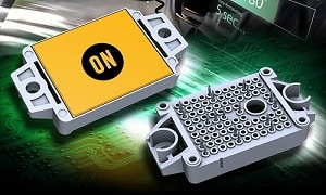
Strengthening the challenging scenario of the current electric vehicle (EV) market is a pair of new 1200 V full silicon carbide (SiC) MOSFET 2-PACK modules by ON Semiconductor.
Based upon planar technology and suited to a drive voltage in the range of 18-20 V, the new 1200 V M1 full SiC MOSFET 2 pack modules are simple to drive with negative gate voltages. The larger die reduces thermal resistance compared to trench MOSFETs, thereby reducing die temperature at the same operating temperature.
Configured as a 2-PACK half-bridge, the NXH010P120MNF is a 10mohm device housed in an F1 package while the NXH006P120MNF2 is a 6mohm device in an F2 package. As the packages feature press-fit pins, they are ideal for industrial applications. An embedded negative temperature coefficient (NTC) thermistor facilitates temperature monitoring.
The new SiC MOSFET modules are now a part of ON Semiconductor’s EV charging ecosystem and can work alongside driver solutions such as the NCD5700x devices. The recently introduced NCD57252 dual channel isolated IGBT/MOSFET gate driver offers 5kV of galvanic isolation and can be configured for dual low-side, dual high-side or half-bridge operation.
Housed in a small SOIC-16 wide-body package, the NCD57252 accepts logic level inputs of 3.3 V, 5 V and 15 V. The high current device (source 4.0 A / sink 6.0 A at Miller plateau voltage) is suitable for high-speed operation as typical propagation delays are 60ns.
Complementing the new modules and gate driver are the ON Semiconductor SiC MOSFETs that provide superior switching performance and enhanced thermals, which results in improved efficiency, greater power density, improved electromagnetic interference (EMI) and reduced system size and weight.
The recently-announced 650 V SiC MOSFETs employ a novel active cell design combined with advanced thin wafer technology that enables a best-in-class figure of merit (FoM) for (RDS(on)). Devices in the series such as the NVBG015N065SC1, NTBG015N065SC1, NVH4L015N065SC1 and NTH4L015N065SC offer the lowest RDS(on) in the market for D2PAK7L / TO247 packaged MOSFETs.
The 1200 V and 900 V N-channel SiC MOSFETs feature a small chip size that reduces device capacitance and gate charge (Qg – as low as 220 nC), reducing switching losses when operating at the high frequencies demanded by EV chargers.


Electric Vehicles are on trending now and changing them is actually a headache for many. Great news, that we can now charge it much faster. Thanks for sharing this news.