


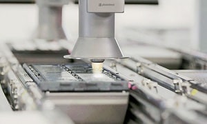
With a dual-lane concept, the developed conveyor belt transports two filled trays to defined positions where the plasma treatment takes place
In the current situation of short supply of semiconductors, it is important to increase the throughput just as it is important to increase the yield for delivering a high-quality product.

To tackle this demand, Plasmatreat GmbH from Steinhagen, Germany, has developed a fully automated inline system for selective pretreatment with Openair-Plasma that is designed according to market requirements. This will benefit customers to implement a flexible, potential-free, high-speed treatment.
The Openair-Plasma process is different from the traditional vacuum plasma process that has been used in semiconductor manufacturing over the years. The offering by Plasmatreat facilitates a fast, inline process for pretreatment under atmospheric conditions that is suitable for surface treatments such as microfine cleaning, activation and plasma coating. For example, it enables microfine cleaning in the packaging processes, thereby replacing the vacuum chamber in the production of chip packaging efficiently and cost-effectively. Other application areas include wire and die bonding, thermal compress bonding and pre-moulding.
Use case
As per a customer request, a special system known as Plasma Treatment Unit (PTU) was developed. A dual-lane concept for this PTU allowed components to be treated parallelly on two conveyor belts within a single system. This PTU can selectively pre-treat JEDEC trays by handling 8 to 128 components on defined depositing devices and for the subsequent thermal compress bonding process, providing maximum throughput.
“Since we already produce fully automated systems for other industries, we already had the internal design and automation expertise required to develop and implement this customer system,” said Nico Coenen, Market Segment Manager Electronics at Plasmatreat.
Because the PTU offers various kinematics and automation options, such as precise-fit handling of assemblies and components, and allows efficient surface treatment, it can be seamlessly integrated into production lines.
“In order to develop an inline-capable system for the semiconductor industry and be able to guarantee the highest possible cycle times, we had to take several process steps into account and implement these with precision as early as the conception phase,” explained Nico Coenen, Market Segment Manager Electronics at Plasmatreat. For example, Plasmatreat developed the dual-lane concept specifically for the high-speed treatment of up to 1.5 m/s. The dual-lane concept is essentially suitable for various applications, with the system designed for both JEDEC trays and lead frames. It has different processing concepts according to the cycle time, and communication within the production line takes place via the standard equipment interface protocol interface in the semiconductor industry, SECS/GEM.
The work steps get recorded in the PTU and the traceability of the treatment is ensured by reading barcodes on the chips. This allows one to detect exactly where and how the individual components were selectively treated, for example, only the top of a component was treated with plasma or not.
