


ATmega16 is an 8-bit high performance microcontroller from the Atmel’s Mega AVR family. Atmega16 is a 40 pin microcontroller based on enhanced RISC (Reduced Instruction Set Computing) architecture with 131 powerful instructions. It has a 16 KB programmable flash memory, static RAM of 1 KB and EEPROM of 512 Bytes. The endurance cycle of flash memory and EEPROM is 10,000 and 100,000, respectively. Most of the instructions execute in one machine cycle. It can work on a maximum frequency of 16MHz. ATmega16 pin diagram should clarify things a bit.
ATmega16 pin diagram
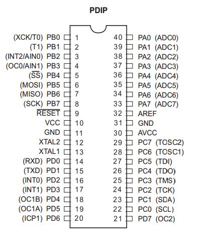
There are 32 I/O (input/output) lines which are divided into four 8-bit ports designated as PA, PB, PC and PD. ATmega16 has various in-built peripherals like USART, ADC, Analog Comparator, SPI, JTAG etc. Each I/O pin has an alternative task related to in-built peripherals. The following table shows the pin description of ATmega16.

ATmega16 Pin description
| PIN1 | I/O , T0 ( Timer0 External Counter Input) ,XCK : USART External Clock I/O |
| PIN2 | I/O, T1 (Timer1 External Counter Input) |
| PIN3 | I/O, AIN0: Analog Comparator Positive Input , INT2: External Interrupt 2 Input |
| PIN4 | I/O, AIN1: Analog Comparator Negative Input, OC0 : Timer0 Output Compare Match Output |
| PIN9 | Reset Pin, Active Low Reset |
| PIN10 | VCC=+5V |
| PIN11 | GND |
| PIN12 | XTAL2 |
| PIN13 | XTAL1 |
| PIN14 | (RXD) ,I/O PIN 0,USART Serial Communication Interface |
| PIN15 | (TXD) ,I/O Pin 1,USART Serial Communication Interface |
| PIN16 | (INT0),I/O Pin 2, External Interrupt INT0 |
| PIN17 | (INT1),I/O Pin 3, External Interrupt INT1 |
| PIN18 | (OC1B),I/O Pin 4, PWM Channel Outputs |
| PIN19 | (OC1A),I/O Pin 5, PWM Channel Outputs |
| PIN20 | (ICP), I/O Pin 6, Timer/Counter1 Input Capture Pin |
| PIN21 | (OC2),I/O Pin 7,Timer/Counter2 Output Compare Match Output |
| PIN22 | (SCL),I/O Pin 0,TWI Interface |
| PIN23 | (SDA),I/O Pin 1,TWI Interface |
| PIN24-27 | JTAG INTERFACE |
| PIN28 : | (TOSC1),I/O Pin 6,Timer Oscillator Pin 1 |
| PIN29 : | (TOSC2),I/O Pin 7,Timer Oscillator Pin 2 |
| PIN30 : | AVCC (for ADC) |
| PIN31 : | GND (for ADC) |
| PIN33 – PIN40 | PAx: I/O,ADCx (Where x is 7 – 0) |
Data sheet for the ATmega 16 is available here. If you have one lying around, some sample circuits to work on, are available here.

thanks for the great informaton sir