


The method enables prototyping and testing of new designs much faster while reducing developing costs by great extent
Wearable sensors ranging from adhesive skin bandages to stretchable implants on organs monitor health or diagnose illnesses and are of
huge help for gathering medical data from patients over extended time periods.

Photolithography, is a standard, multistep process that uses light to create patterns on semiconductors for fabricating PCBs and microprocessors. Often done in clean rooms to avoid even a speck of dust ruining the fabrication, the process is quite expensive, which also involves a US$200 vinyl cutter.
Now, engineers at UC Berkeley have developed a new technique for making wearable sensors that enables prototyping and testing of new designs much faster while cutting costs by almost 75%.
“Most researchers working on medical devices have no background in photolithography,” said Renxiao Xu, lead researcher of the technique, who developed it in 2020 while pursuing his PhD in mechanical engineering at Berkeley. “Our method makes it easy and inexpensive for them to change their sensor design on a computer and then send the file to the vinyl cutter to make.”

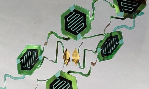
Wearables consist of flat wires (interconnects) as well as sensors, power sources and antennas to communicate data to smartphone apps or other receivers. To maintain full functionality, the tissue upon which they are placed must stretch, flex and twist without straining the electronic circuitry. For this, an “island-bridge” structure is used wherein all the electronics are housed on different islands that are connected to each other through bridges. Their spiral and zigzag shapes stretch like springs to accommodate large deformations.
Traditionally, these island-bridge systems have been built using photolithography that requires a clean room and sophisticated equipment. With the new technique, the process can be realised in a faster and more economical way, especially when making the one or two dozen samples that medical researchers typically need for testing.
The island-bridge sensor development starts by attaching an adhesive sheet of polyethylene terephthalate (PET) to a Mylar (biaxially oriented PET) substrate. Other plastics would also work. A vinyl cutter then shapes them via a tunnel cut that slices through only the top PET layer but leaves the Mylar substrate untouched and via a through cut that carves through both layers.
Sensor elements are then attached to the contact pads present on the islands. For electronic devices, such as resistors, a conductive paste and a common heat plate are used to secure the bond. Lab-synthesised components, such as carbon nanotubes, can also be applied directly to the pads without any heating. Once this is done, the vinyl cutter carves the sensor’s contours, including spirals, zigzags and other features.
To demonstrate the technique, a variety of stretchable elements and sensors were devised. One of them included a sensor that was placed the human under the nose to measure human breath based on the small temperature changes.
“For a breath sensor, you don’t want something bulky,” said Liwei Lin, professor of mechanical engineering and co-director of the Berkeley Sensor and Actuator Center. “You want something thin and flexible, almost like a tape beneath your nose, so you can fall asleep while it records a signal over a long period of time.”
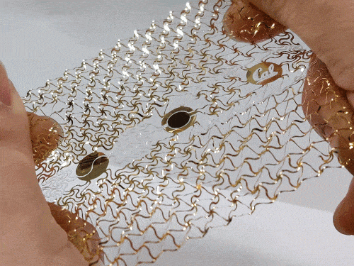
Another prototype consisted of an array of water-resistant supercapacitors that stored electrical power like a battery but released it more rapidly.
“We could also make more complex sensors by adding capacitors or electrodes to make electrocardiogram measurements, or chip-sized accelerometers and gyroscopes to measure motion,” Xu said.
Size is sensor cutting’s one key limitation. Its smallest features are 200 to 300 micrometres wide, while photolithography can produce features that are tens of micrometres wide. But most wearable sensors do not require such fine features.
The researchers believe this technique could one day become imperative for studying wearable sensors or new diseases. Prototypes could be designed using high-powered computer-aided design (CAD) software or simpler apps made especially for vinyl printers.
