
So far, electronics has depended heavily on silicon for its development. But now recent developments in material science and new techniques are emerging to take electronics further…
The era of electronics started much before it got its name as electronics. Earlier it was called radio engineering. The electronic word came into vogue in late 1940 and became prominent by the late 1950s. The electronics industry was revolutionized by the invention of the first transistor in 1948, which was a Germanium-based semiconductor. However, germanium has the drawback of breaking down at around 80°C, so most of it is now silicon.

Now, for more than seven decades, we have been living with electronics hand in hand. Our reliance and dependency on it are increasing day by day and we have come to an era where without electronics we cannot survive.
For decades and decades together, silicon has remained the only option for electronics. And we have seen the performance of silicon-based devices in terms of speed, power consumption, size, and cost improving multi-fold. But recent developments in material science are paving new ways to electronics.
Recent Developments in Material Science
- 2D Electronics
- Organic Electronics
- Memristors
- Spintronics
- Molecular Electronics
2D Electronics
In the year 2010, Nobel Prize for Physics was awarded to Andre Geim and Konstantin Novoselov for the experiments carried out on graphene, which is a structural variant of carbon. Carbon atoms in graphene form a hexagonal two-dimensional structure (lattice), which is as thick as an atomic layer and has high electrical conductivity, high thermal conductivity, high mechanical flexibility, and probably the highest mechanical strength (strongest material tested ever). Graphene is from where the concept of two-dimensional (2D) electronics started.
A 2D semiconductor used in two-dimensional electronics has its thickness in an atomic scale. It has only length and breadth, as its third dimension of thickness is almost missing. This semiconductor can conduct more electricity and heat, consumes lesser power, and exhibits greater mechanical strength and stability.
2D materials are incredibly thin and lightweight and are stable at sizes below 10nm (1nm=10–9 meters), the point at which traditional semiconductor materials start failing. Graphene is also highly transparent to the incident light, and it absorbs only 2% of the light incident upon it.
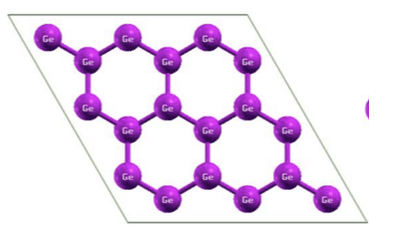
Graphene poses some technical challenges while being used in digital electronics (because at the atomic level, it has a lack of band gap). Going forward into the domain of material science, nano-layers of material of the same group—such as Si, Ge, and Sn—exhibit similar properties as graphene and have no lacking while being used in digital electronics. Thus, 2D electronics, which got their origin in graphene, have moved into other materials like silicine, germanene, and phosphorene. These materials have additional advantages like excellent magnetic properties, tuneable band gaps, active optical properties, and so on.
2D materials like silicine, germanene, and phosphorene have tremendous potential in the field of optoelectronics as light-emitting diodes (LEDs), optical signal processors, and solar photovoltaic panels. Owing to their lightweight and flexibility they are also suitable for flexible design of wearables and other flexible devices.
2D materials can be used to produce a transistor equivalent to the size of a molecule. The size and stability of these pave the way for their use in computing. The most promising application of 2D electronics is in the solar energy industry, where any surface like paper, walls, windows, a glass of consumer durables, and so on can be converted into solar cells. 2D electronics find its use in supercapacitors, fuel cells, and more.
Organic Electronics
In the year 2000, the Nobel Prize for Chemistry was given to Alan Heeger, Alan Macdiarmid, and Shirakawa for the development of conductive polymers. In common parlance, they proved that even plastic can conduct electricity. This paved the origin of organic electronics. Organic electronics materials are made of organic molecules (carbon-based materials) or polymers by chemical synthesis. Organic electronics materials also include a variety of dyes and other organic molecules.
Organic materials are yet to compete in performance if compared with conventional inorganic conductors and semiconductors, but they come with several advantages over conventional ones. They have low material cost as well as production cost, have adaptivity of synthesis, are bio-compatible, and are mechanically flexible.
We already are familiar with the organic LED (OLED) screens for our smartphones and TV sets. But their potential for future application stretches far beyond. Organic material enables us to fold our smartphones or other portable devices like paper.
Healthcare systems will see new possibilities that organic materials offer, where they can interact with our biological cells and sensory organs. Healthcare systems can respond to signals at the cellular level in our body with the capability added by organic electronics. Owing to this possibility, our artificial organs or limbs can work very near to the natural in terms of feeling and reaction. Artificial skin that is close to natural skin is not very far off.
Organic electronics unleash the possibility of printing solar cells over plastic sheets that can be folded like a map, ready to be installed anywhere. As the organic electronics materials will be synthesized in the lab and will be bio de-gradable, they will have a better sustainability cycle when compared to conventional materials, which have a dependency on mined materials from the earth.
Memristors
The word memristor has been derived from the two words: memory and resistor, meaning thereby that it is a resistor with memory. In theory, memristors were predicted as early as 1971 by Leon Chua and were explained through some mathematical equations. The prediction said that we were missing an electronic component like a memristor. But the device was physically produced much later in 2008 by Stanley Williams.
The resistance of a memristor can be programmed and at the same time, the device memorizes its value. Recent developments in memristors have made them very reliable as they can be cycled more than 100 billion times and can remain stable for more than 10 years.
We are very much familiar with random access memory (RAM) and flash memory (such as in pen drives). In RAM, memory mobility is very high, but the disadvantage is that it does not retain the data in power-off mode. Flash drive retains the data in power-off condition, but their memory mobility is very slow. Memristor combines the capability of both, as it has very high mobility and also retains the data even in the power-off mode.
Memristor, when compared with a conventional solid-state device, requires less energy and has a faster speed of operation. At the same time, a memristor can accommodate double the data in the same physical size of the device compared to a conventional semiconductor. Not only that, but our conventional semiconductors, when exposed to radiation, either lose the data or the data is distorted, whereas memristors are immune to the radiation.
In our conventional computing systems, data is stored in a location (memory) and processed in another location (processor). The data traffic between these two locations reduces the speed of computation and at the same time consumes a huge amount of energy. Memristors store and process the information in the same location. Due to this fact, the challenge of speed, as well as power consumption, is taken care of. Hence, the use of memristors in our conventional computing is paving a new way.
The property of memristors to store and process information at the same location is like that of the human brain’s building blocks—neurons. With this capability, there is a paradigm shift in computing, called neuromorphic computing, which will mimic our internal neuron structure and energy-efficient processing like our brain. This will lead to putting a brain to a chip, that is, embedded artificial intelligence in the hardware itself, doing away with the need to run it on a separate software platform.
In the context of artificial intelligence (AI), neuromorphic computing by memristors will lead to a new generation of chips, which will be able to do self-learning and interpret the environment around it, without the help of coded software. Currently, AI runs on the cloud. With this neuromorphic computing, the AI running in central servers on the cloud will shift to the chip itself as edge computing.
In practical terms, an autonomous car requires network connectivity (4G/5G) through which it sends the data collected through its sensors to its central server on the cloud for analysis. The central server does the data analysis and sends the execution command back to the car. In this process, latency is created and it is also very power-consuming to handle such huge data. With the advent of memristors, all computations can be done locally inside the brain of the car. This will take AI to a different level.
Neuromorphic computing will establish a new level of AI in edge computing, robotics, the Internet of Things (IoT), machine vision, artificial skin, sensory organ, and so on.
Spintronics
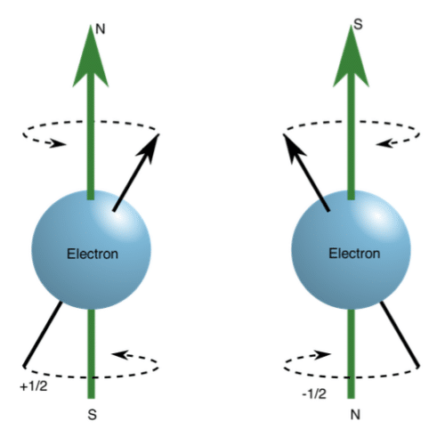
Spintronics is a word coined from the words spin and electronics. The invention of this can be traced back to early 1988 when the giant magnetoresistive (GMR) effect was discovered by Albert Fert in France and Peter Gruenberg in Germany. Our conventional electronics harness the property of charge on the electrons, whereas spintronics harnesses the property of spinning the electrons.
Conventional electronics and semiconductors define the state of a device as zero and one state. For example, a capacitor is said to be in a ‘one’ state when it is fully charged and in a ‘zero’ state when fully discharged. This is how our data is stored in ‘0’ and ‘1’ format in our memory devices with the help of billions of capacitors.
Apart from the charge on the electron, every electron spins on its axis in two different directions—clockwise and counter-clockwise. This motion is inherent to electrons and can be altered from one to another with some application. This spinning of electrons generates a magnetic moment that can be altered with the application of an external magnetic field. Spintronics uses this property of electrons where clockwise rotating electrons are said to be in the ‘0’ state and counter-clockwise in the ‘1’ state.
In a conventional way, charging and discharging of capacitors is power-consuming. In order to maintain the state of a capacitor in the ‘1’ state, it has to be charged several times in a second, whereas the spin of an electron is inherent and it does not require any power to maintain the same. The advantage of this is that it is non-volatile, which means the memory does not go off when the power is shut down, which is the problem in conventional charge-based electronics.
Spintronics is the driving technology for next-generation nanotechnology. It will enhance memory capability and processing speed while reducing power consumption. Quantum-mechanical computing based on spintronics can achieve a speed unheard of with conventional electrical computing.
The spinning of electrons, which is the fundamental of spintronics, can be managed in several ways, such as by applying:
- Magnetic field
- Stray electric and magnetic field
- Electromagnetic waves, for example, circularly polarised light
- A thermal gradient
While spintronics is a magnetic phenomenon of electrons, ferromagnetic material started as a core to this, and different devices like giant-magneto-resistance, tunneling-magneto resistance, and magnetic-tunnel-junction are built around it. Despite paced advancement in ferrous material, semiconductor spintronics is also part of a focus to find a way to generate and control the spins of the electrons.
The selection of material for semiconductor spintronics depends on the property of material exhibiting ferromagnetism at room temperature, for example, gallium arsenide (GaAs) and indium arsenide (InAs). The spinning of electrons can be easily controlled and managed in semiconductors and such devices can be easily integrated with present semiconductor architecture and technology. Based upon spintronics we have devices like spin-transistors, spin-LEDs, optical switches, memory devices, and so on.
Because of the unique science behind this technology, the operation of spintronics sensors and devices is more precise, reliable, and repeatable. Compared to electromechanical sensors, spintronics sensors are immune to mechanical shock, vibration, and temperature. Due to these very precise properties, the sensors are being used in Class I medical device hearing aids and provide miniaturization, stability, and ease of operation with better sensitivity. Spintronics devices and sensors are also used in Class III devices like pacemakers and implants, where all the above properties are the key to their use.
Spintronics devices are being used to detect diseases in the human body, like cancers. The fact that the affected organ has different magnetic properties than the normal one is being harnessed in this detection. And this is being used as a major game changer in the medical field. Electron transport in DNA is another field of great importance and research that is being carried out.
Spintronics devices are also used in mass storage. The storage density, which is the amount of data stored in a physical area of a chip, is much higher than the conventional one. For example, it can store more than one trillion bits per square inch. Another game changer of the future may be the spin-based quantum computation in nanotechnology, where neuromorphic computing and quantum computing will take the front seat.
Molecular Electronics
The goal of electronics is miniaturization. Molecular electronics is that branch of electronics, or for that matter research, where a single molecule or a bunch of molecules is treated as electronics building blocks. Whereas our conventional electronics are based on the bulk of the material, in single-molecule electronics – that is, molecular electronics – this bulk of the material is replaced with a single molecule.
Molecular electronics as a potential technology is basically a bottom-up approach where the smallest building unit, a molecule, is assembled to perform the electronic operation. Whereas, the top-down approach is to shrink macroscopic components and systems.
The origin of molecular electronics can be traced back to 1974 when Mark Ratner and Arieh Aviram published the study of electron transport through a single molecule. Their suggestion of an ad-hoc calculation and the proposal that a single molecule could be used as a device has led to this branch of electronics.
Electron movement by a single molecule is at the center of molecular electronics. This concept of electron movement through a single molecule is described in two different ways. One way is the movement of an electron through a single molecule, which is described as electron transfer. The other is the movement of current passing through a single molecule.
In molecular electronics, the goal of miniaturization is achieved and due to this power consumption for its operation reduces drastically, whereas its sensitivity increases exponentially. Another major advantage of molecular electronics is that some of the molecular systems have the tendency to self-assemble to a bigger functional block. In this phenomenon, the components of a system come together spontaneously due to some environmental factor to form a large functional unit.
The dimensionally small molecular circuit or electronic component has a wide range and variety of electrical, mechanical, optical, and thermal properties. And each of these properties in singular as well as in combined state gives rise to countless new physical phenomena.
Molecular electronics, in principle, offers the following advantages over conventional electronics:
- The reduced size of each building block—the molecule—will offer a higher packing density for the devices. This will subsequently reduce the cost and power and improve efficiency and effectiveness.
- Molecular wire could reduce the transit time of a transistor, thereby reducing the time of operation.
- Molecular self-assembly can be used to modify the electronic behavior of an electronic component to provide both switching and sensing capability on a molecular scale.
- Special properties of a molecule, such as stable geometric structure, could lead to a new dimension in electronics, which is otherwise not possible in conventional electronics.
- By intelligent choice of composition and geometry, one can create variation in molecular transport, binding, optical, and structural properties.
But molecules have the obvious disadvantage of being unstable at high temperatures. Moreover, the fabrication of a reliable molecular junction requires control at unprecedented levels. Achieving the same is not only difficult but slow and costly too.
Several molecular electronic solutions have already been developed, such as molecular wire, single-molecule transistors, rectifiers, and so on. However, molecular electronics is still in the infant stage of research and these devices are yet to come out of laboratory bed.
Rajesh Jha is a Senior Leader and a Strategic Expert offering 28 years of rich experience in propelling business profitability and growth and driving operational excellence by way of Strategic Management, Lean Manufacturing, implementation of Best Operational Practices, and driving People Management Initiatives. He is associated with VVDN Technology as
V.P. (Manufacturing)