




As semiconductor manufacturing takes shape in India, the materials connecting and packaging chips are facing their own set of challenges and opportunities.
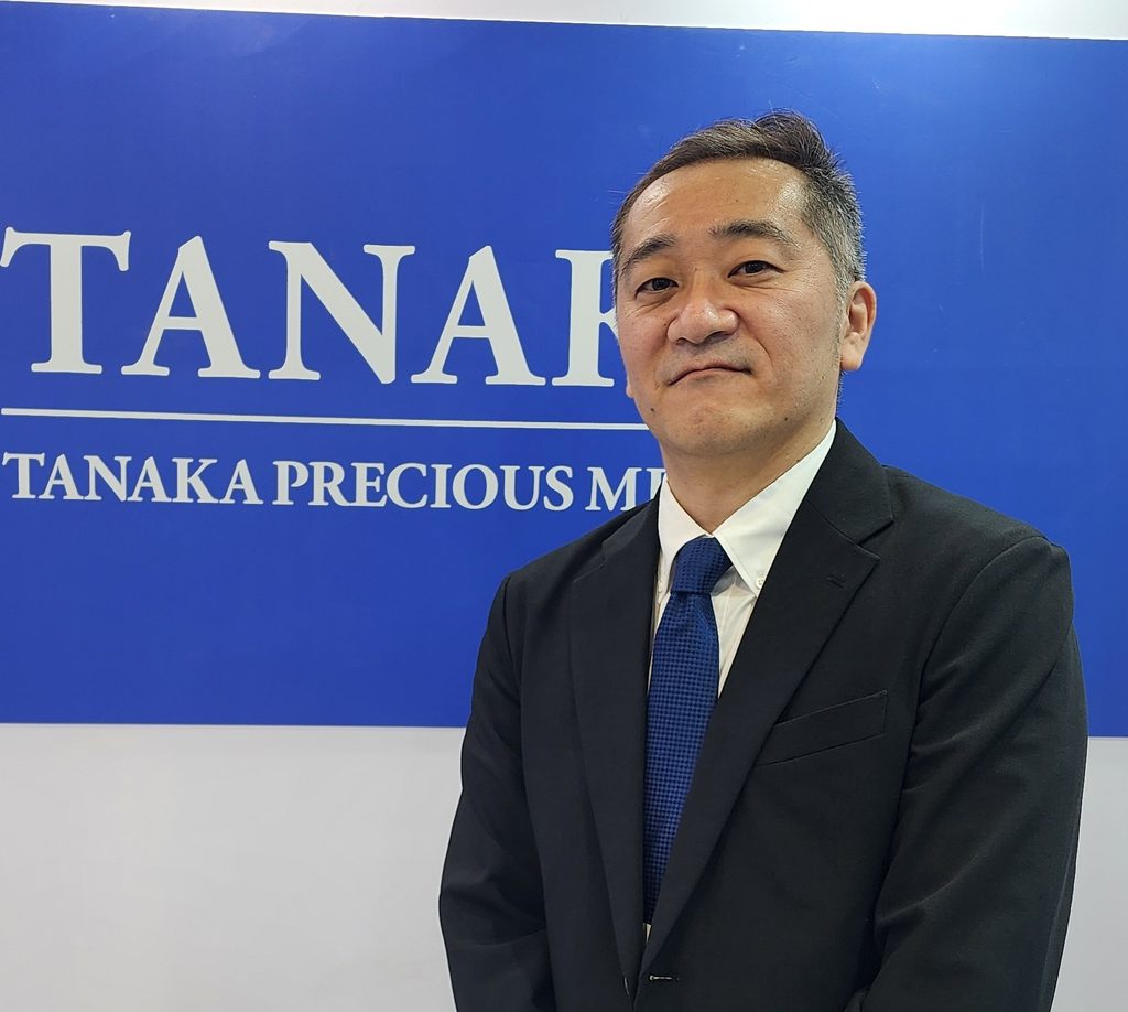
At Semicon India, EFY interacted with Kazuo Meguro, Managing Director, TANAKA PRECIOUS METALS INDIA PRIVATE LIMITED, to understand how the company is responding to the changing material requirements of semiconductor manufacturing and what it sees ahead for India. One area attracting attention is the continued dependence on precious metals such as gold and silver. Rather than treating this simply as a cost challenge, TANAKA is exploring alternative materials and specialised alloys that could reduce dependence on precious metals while retaining the properties required for semiconductor applications.
At the same time, the company is seeing semiconductor projects in India move from sampling towards mass production, which could significantly increase material requirements. This also raises the question of localisation. The company currently supplies the Indian market through its overseas manufacturing network, but has received requests from customers for local production. The company is monitoring demand and production volumes before deciding whether to establish manufacturing in India.
Beyond manufacturing, the company is also looking at issues such as supply-chain resilience, logistics,cs and the recovery of precious metals as semiconductor production expands. What makes this interesting is that the semiconductor manufacturing challenge is not limited to fabs and packaging equipment. The materials themselves are becoming part of the innovation equation. Their work on material alternatives, their approach to supply security, and their thinking around possible manufacturing in India point to a less visible but important part of the country’s semiconductor build-out.
The full EFY interview, where it sees the next material challenges and what could change as India’s semiconductor ecosystem moves towards scale,le will be uploaded soon.
