


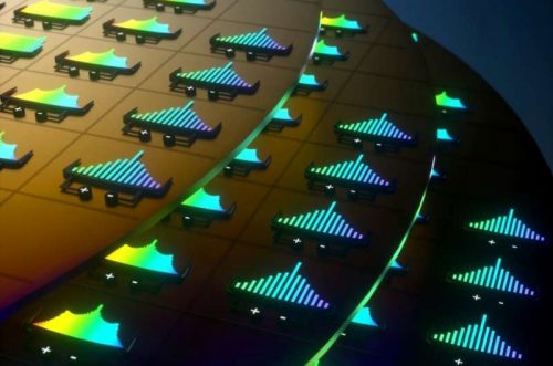
The wafer-scale process enables thousands of devices to be made from a single 100-mm-diameter wafer by producing a laser microcomb.
Researchers from The Bowers lab along with the Kippenberg lab have developed an integrated on-chip semiconductor laser and resonator capable of producing a laser microcomb.

This new technology in which light can travel in the waveguide without losing a significant amount of its intensity gives scope for commercially scaled production. Due to its capability to make thousands of devices from a single wafer using industry-standard complementary metal-oxide-semiconductor (CMOS)-compatible techniques, this technology enables semiconductor lasers to be seamlessly integrated for long-distance optical communication. “Our approach paves the way for large-volume, low-cost manufacturing of chip-based frequency combs for next-generation high-capacity transceivers, data centres, space and mobile platforms,” the researchers stated.
The success of this study was published in a paper titled “Laser soliton microcombs heterogeneously integrated on silicon,” in the new issue of the journal Science.
“The field of optical comb generation is very exciting and moving very fast. It is finding applications in optical clocks, high-capacity optical networks and many spectroscopic applications,” said Bowers, the Fred Kavli Chair in Nanotechnology and the director of the College of Engineering’s Institute for Energy Efficiency. “The missing element has been a self-contained chip that includes both the pump laser and the optical resonator. We demonstrated that key element, which should open up rapid adoption of this technology.”
The Background
A method integrating a laser onto a silicon wafer was pioneered by professor John Bowers who leads the Bowers Lab, and the technology has since been widely used in combination with other silicon photonics devices. This method has extensively increased energy efficiency by replacing the copper-wire interconnects that formerly linked servers at data centres.
After several years of collaboration with Bower the group from the Swiss Federal Institute of Technology (EPFL), headed by Tobias J. Kippenber discovered “microcombs,” a series of parallel, low-noise, highly stable laser lines. Each of the many lines of the laser comb can carry information, extensively multiplying the amount of data that can be sent by a single laser.
Microcombs
The technology of microcombs finds its applications in optical metrology and sensing, optical communications, LiDARSs, and astrophysical studies.
Microcombs are optical frequency combs that emit mutually coherent laser lines that have constant phases relative to each other. The working principle is rather simple to explain. A single laser line produced by a distributed feedback (DFB) laser passes through an optical phase controller and enters a micro-ring resonator. As the light propagates around the ring, the intensity of power increases. When the power intensity reaches a certain threshold, nonlinear optical effects occur which causes one laser line to create two additional, identical lines on either side. Each of those two “sidelines” creates others, leading to a cascade of laser-line generation. “You end up with a series of mutually coherent frequency combs and a vastly expanded ability to transmit data,” said Chao Xiang, lead author of this study.
Using the “photonic damascene process” and UCSB’s heterogeneous integration process, it was possible to develop high-performance lasers on silicon substrate along with a record low-loss, high-Q silicon nitride micro-resonators. The wafer-scale process enables thousands of devices to be made from a single 100-mm-diameter wafer, a production-level that can be scaled up further from the industry-standard 200-mm- or 300-mm-diameter substrate.
“I think this work is going to become very big,” said Xiang. “Future silicon photonics using co-packaged optics will likely be a strong driver for higher-capacity transceivers using a large number of optical channels.”