Table of Contents
Logic gates are the basic building blocks of digital electronics. More common ones being the OR, AND, NOR, NAND, EX-OR and NOT gates. Typically, a gate takes input from two input terminals, performs some operation and outputs the result at an output terminal. The NOT gate, however lacks the second input. It consists of only one input and one output. A NOT gate is used to output the Boolean inverse of the applied input. Hence the name ‘Digital Inverter’ or ‘Inverting buffer’. The most commonly used NOT gate IC is the 7404.
NOT Gate Logic Symbol and Boolean Expression
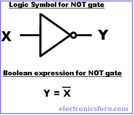
As NOT gate IC is an inverter, the output is represented by a “ ͞ “ (bar) symbol over the input. The Boolean expression can be written as Y = X͞. That is, if X is the input and Y is output, then output Y equals to X͞, not X. In other words, when X=0, Y =1 and vice versa.
The bubble in the symbol for a NOT gate at the output port represents the inverting operation. That means for a high logic signal input, the output of the NOT gate IC will be LOW. Similarly for LOW logic signal input, the output of NOT gate IC will be HIGH.

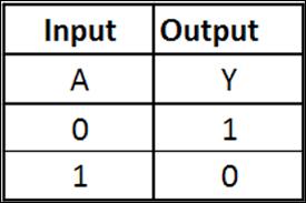
Truth Table for NOT gate IC
“If X is NOT true, then Y is true”
Recommended Operating Conditions of NOT Gate IC 7404
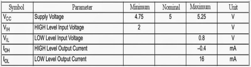
Recommended operating conditions of 7404 NOT gate IC are given in the following table. Ideally, the supply voltage should range between 5.25V and 4.75V. A voltage greater than 2V will be considered as HIGH (1) and voltage less than 0.8V will be considered as LOW (0).

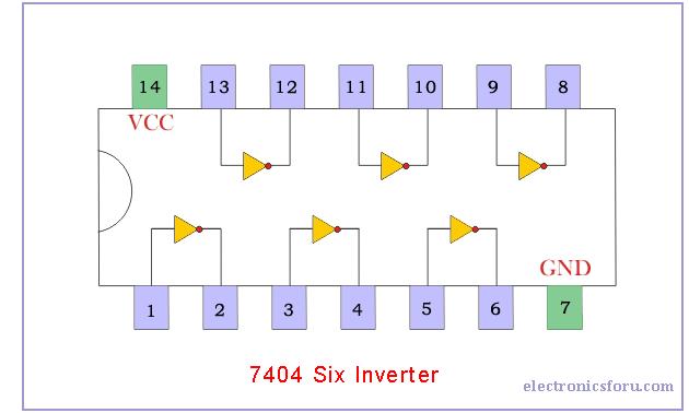
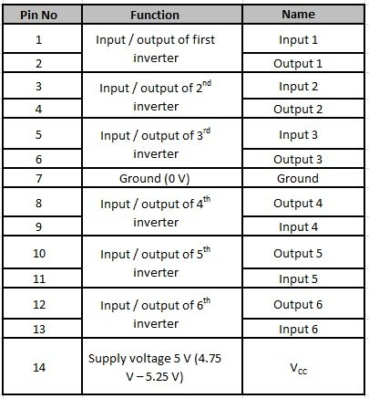
Pin-Out Diagram of 7404 NOT Gate IC
Each 7404 NOT gate IC has 6 NOT gates arranged as shown in the following figure. 14th pin is the Vcc and the 7th pin is the Ground. The outputs directly interface to CMOS, NMOS and TTL. It supports wide operating conditions and has large operating voltage range.
The datasheet for NOT gate IC 7404 is available at 7404 IC datasheet.
NOT gate is however just on of the 7400 series. For the 7400 series tutorial, turn over to next page.
7400 Series Tutorials
7400 series is an extended family of digital integrated circuits. Chips in this series include a variety of discrete logic chips such as AND gates, OR gates along with a variety of registers, decoders, and RAM units.
7400 series main features
Some of the main features and specifications for the 7400 series logic family are detailed below
|
PARAMETER |
SPECIFICATION |
|
Supply Voltage |
Normal 5 V (4.75 – 5.25) |
|
Propagation delay per gate |
Typically 10 ns |
|
Max toggle speed |
25 MHz |
|
Power consumption per gate |
10 mW |
Using a 7400 family IC, an engineer can design logic gates, flip-flops, counters, and buffers in individual packages and wire them together as desired to solve a specific problem. Some most common members of the 7400 family and their functions are,
|
DEVICE NUMBER | DESCRIPTION |
|
7400 |
Quad 2-input NAND gate |
|
7402 |
Quad 2-input NOR gate |
|
7404 |
Hex Inverter |
|
7408 |
Quad 2-input AND gate |
|
7432 |
Quad two-input OR gates |
|
7447 |
BCD to seven-segment display decoder/driver |
|
7474 |
Dual D-type positive edge triggered flip-flops |
|
7470 |
Four-bit decade counter |
|
7486 |
Quad 2-input XOR gate |
|
7490 |
Four-bit decade counter |
|
74138 |
Three-to-eight decoder |
|
74153 |
Dual 4-to-1 multiplexer |
|
74157 |
Quad D-type flip-flops with complementary outputs |
|
74160 |
Four-bit binary synchronous counter |
|
74164 |
Eight bit parallel out serial shift register |
|
74174 |
Quad D-type flip flops with complementary outputs |
|
74193 |
Four-bit synchronous up/down binary counter |
|
74245 |
Octal bus transceiver with tri-state outputs |
|
74266 |
Quad 2-input XNOR gate |
|
74373 |
Octal D-type transparent latch |
| 74374 |
Octal D-type flip-flops |
These are just a few of the full set of 7400 family members. Other IC’s among 7400 series are no longer used as their specific function is rarely required as a separate chip in modern digital electronics designs. However, the parts listed above, and many others that are not listed, are still easily available today and are commonly found in a broad range of digital designs ranging from low-end to high-tech devices.
IC 7400, NAND gate
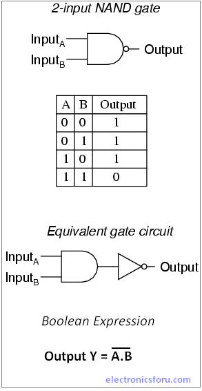
7400 IC is the most widely used TTL (Transistor-Transistor Logic) device in the world. It contains four independent two-input NAND gates. Its popularity is based on the fact that any logic gate function can be created using only NAND gates. Therefore, 7400 is ideal for learning about digital logic as well as a “universal spare” when certain logic functions are needed.
The NAND (Not – AND) gate has an output that is normally HIGH (1) and only goes LOW (0) when all of its inputs are HIGH (1). The Logic NAND Gate is the reverse or “complementary” form of the AND gate.
The logic or Boolean expression for a logic NAND gate is that for Logical Addition, which is the opposite to the AND gate. The Boolean expression for a logic NAND gate is denoted by a single dot or full stop symbol, (.) with an over line or bar, ( ‾ ) over the expression to signify the NOT or logical negation of AND gate.
Commonly used AND gate IC is 7400. It has four independent NAND gates with standard pin configuration. The operating temperature is 70 degree celsius.
IC 7402, NOR gate
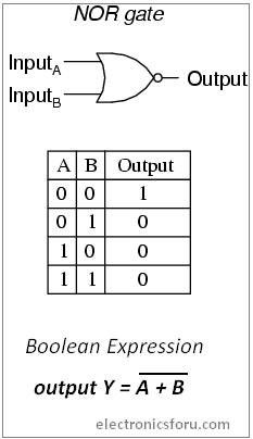
The NOR gate is a digital logic gate that implements logical NOR. A HIGH output (1) results if both the inputs to the gate are LOW (0), if one or both input is HIGH (1), a LOW output (0) results. NOR is the result of the negation of the OR operator. It can also be seen as an AND gate with all the inputs inverted. NOR is a functionally complete operation because the NOR gates can be combined to generate any other logical function. It shares this property with the NAND gate. The truth table Boolean expression and the symbol of a NOR gate are below.
The commonly used NOR gate IC is IC 7402. It has four 2-Input NOR gates in 14-Pin DIP Package. The special features include large operating voltage range and wide operating conditions.
IC 7408, AND gate
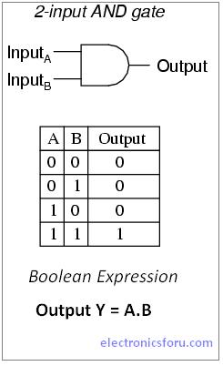
A Logic AND Gate is a type of digital logic gate that has an output which is normally LOW (0) and only goes HIGH (1) when all of its inputs are HIGH (1). The output state of a “Logic AND Gate” only returns “LOW” again when any of its inputs are LOW (0). In other words for a logic AND gate, any LOW input will give a LOW output.
The truth table, symbol and Boolean expression for AND gate are below.
The commonly used AND gate IC is 7408IC. It consists of a four 2-input logic AND gates in a 14-pin DIP package. It supports wide operating voltage range and has wide operating conditions.
IC 7432, OR gate
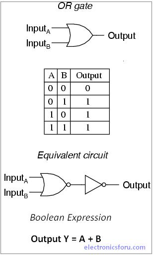
OR gate performs logical OR operation which means output is HIGH (1) if at least one of the inputs is HIGH (1). Just like AND gate, an OR gate may also have two or any more numbers of inputs but only one output. Only if all of the inputs are LOW (0), the output will be LOW (0) and in all other inputs conditions the output will be HIGH (1).
The truth table, symbol and Boolean expression for OR gate are below.
The commonly used OR gate IC is IC7432. It consists of four 2-input OR gates in a 14-pin DIP package. The datasheet for IC 7432 is available at 7432 Technical Datasheet.
IC 7486, XOR gate
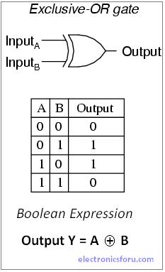
An XOR (Exclusive – OR) gate is a digital logic with two or more inputs and one output that performs exclusive disjunction. The output of the XOR gate is HIGH (1) only when exactly one of its inputs is HIGH (1). If both inputs of a XOR gate are LOW (0), or if both inputs are HIGH (1) , then the output of the XOR gate is false. The symbol, truth table and the Boolean expression for XOR gate are below.
The 7486 IC package contains four independent positive logic XOR GATES. Pins 14 and 7 provide power for all four logic gates.
IC 74266, XNOR gate
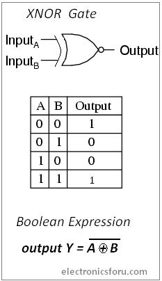
Basically the “Exclusive-NOR Gate” is a combination of the Exclusive-OR gate and the NOT gate but has a truth table similar to the standard NOR gate in that it has an output that is normally HIGH (1) and goes LOW (0) when any of its inputs are HIGH (1).
However, the output goes HIGH (1) only when both of its inputs are at the same logic level, either binary “1” or “0”. For example, “00” or “11”. The truth table, equivalent circuits, Boolean expression and symbol for XNOR gate are below.
The commonly used IC for XNOR gate are the 74266 (Quad 2-input gate with open collector output) and 747266 (Quad 2-input XNOR gate). The IC comprises of four independent 2-input exclusive-NOR gates with open-collector outputs which can be used a 4-Bit digital comparator. The open-collector outputs permit tying outputs together for multiple-bit comparisons.
IC 7447, BCD to seven segment decoder/driver IC
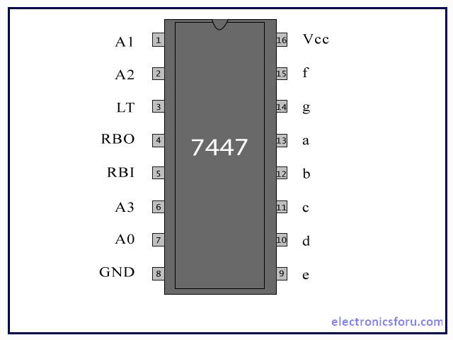
7447 IC accepts a binary coded decimal as input and converts it into a pattern to drive a seven-segment for displaying digits 0 to 9.
Binary coded decimal (BCD) is an encoding method in which each digit of a number is represented by its own binary sequence (usually of four bits).
It accepts four lines of BCD (8421) input data and generates their complements internally. The data is decoded with seven AND/OR gates to drive indicator LEDs of the seven segment display directly. The outputs correspond to common anode (CA) configuration of seven segment. The pin out diagram and the pin description for IC7447 are shown below.
| Pin No |
Function | Name |
|
1 | BCD Input 2 | A1 |
| 2 | BCD Input 3 | A2 |
| 3 | Display test (Active low) | LT |
| 4 | Ripple blanking output (Active low) | RBO |
| 5 | Ripple blanking input (Active low) | RBI |
| 6 | BCD Input 4 | A3 |
| 7 | BCD Input 1 | A0 |
| 8 | Ground (0V) | Ground |
| 9 | Segment outputs; Active low | e |
| 10 | d | |
| 11 | c | |
| 12 | b | |
| 13 | a | |
| 14 | g | |
| 15 | f | |
| 16 | Supply voltage; 5V (4.75V – 5.25V) |
Vcc |
The datasheet for 7447 IC is available at 7447 IC.
More basic articles available in the learning corner.