


Summary:
A low-light solar energy harvesting system using the LTC3105 with built-in MPPT can efficiently extract power from indoor ambient light (as low as a few lux), start from voltages as low as 250 mV, and store energy in a supercapacitor to enable battery-less IoT devices. By continuously operating at the PV cell’s maximum power point, the design significantly improves efficiency (up to ~80–90%), making it ideal for wearables, sensor nodes, and energy-autonomous systems.
Solar energy harvesting is a crucial aspect of many IoT devices, particularly in regions lacking electricity or experiencing an unreliable power supply. Directly harvesting solar energy from a PV cell is often inefficient, especially in indoor environments with ambient light. This is particularly relevant for wearable devices, IoT nodes, and sensor networks that frequently operate under low indoor lighting conditions.
To address this, a specialized energy harvesting system is essential to enhance efficiency and practicality. In this context, we utilize the LTC3105 to harvest solar energy. As per its datasheet, it supports MPPT (Maximum Power Point Tracking), enabling effective energy harvesting even at very low light levels—as low as a few lux.
By employing the MPPT technique, the system dynamically adjusts the load on the PV cell to operate at its maximum power point—the optimal voltage and current combination that maximizes power output (P = V × I) under varying conditions such as light levels, temperature, and shading.

This system harvests energy from a small solar cell and stores it in a supercapacitor, ensuring reliable operation of IoT devices even in dim indoor lighting. The design incorporates MPPT for optimal energy extraction, a low start-up voltage (as low as 250 mV), and integrated features such as output disconnect and a low-dropout (LDO) regulator for auxiliary power.
We will delve into the technical details of the LTC3105, provide an in-depth explanation of MPPT, and explore the circuit design, including component selection for a 3V output suitable for charging a supercapacitor. This approach is ideal for battery-less or energy-autonomous systems, where the supercapacitor serves as a buffer to store harvested energy and supply it during peak demand or low-light periods.
By preventing the input voltage from dropping below the MPPT setpoint, the circuit maximizes efficiency, potentially achieving conversion efficiencies of up to 80–90% in low-light scenarios.
Bill of Material
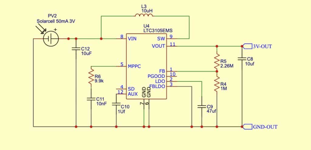
For the main energy harvesting, we use the LTC3105 along with a PV cell as the solar energy receiver. The complete list of components is provided in the table.
| ID | Name | Designator | Footprint | Quantity |
| 1 | 10uF | C3 | CAPACITOR 10UF SMD 0805 | 1 |
| 2 | 10nF | C4 | CAPACITOR 10UF SMD 0805 | 1 |
| 3 | 1Uf | C5 | CAPACITOR 10UF SMD 0805 | 1 |
| 4 | 47uf | C6 | CAPACITOR 10UF SMD 0805 | 1 |
| 5 | 10uf | C7 | CAPACITOR 10UF SMD 0805 | 1 |
| 6 | 10uH | L2 | 10UH INDUCTOR | 1 |
| 7 | Solarcell 50mA 3V | PV1 | 39X39 SOLAR CELL | 1 |
| 8 | 9.9k | R1 | RESISTORS_THROUGHHOLE:RESISTOR_HORIZONTAL_RM10MM-VG | 1 |
| 9 | 2.26M | R2 | RESISTORS_THROUGHHOLE:RESISTOR_HORIZONTAL_RM10MM-VG | 1 |
| 10 | 1M | R3 | RESISTORS_THROUGHHOLE:RESISTOR_HORIZONTAL_RM10MM-VG | 1 |
| 11 | LTC3105EMS | U2 | MSOP-12_L4.0-W3.0-P0.65-LS5.0-BL | 1 |
Solar Energy Harvesting Circuit Design
Here, our design utilizes the Maximum Power Point Tracking (MPPT) technology to efficiently harvest energy. Let’s delve into what MPPT is and how it differs from traditional methods, making it particularly effective for indoor and low-light environments.
MPPT is an optimization technique employed in solar systems to extract the maximum possible power from a photovoltaic (PV) source. The power-voltage (P-V) curve of a PV cell has a peak point where power is maximized.
However, this peak point shifts with environmental changes. To address this, MPPT algorithms or circuits continuously monitor and adjust the operating point by varying the effective load (e.g., through Pulse Width Modulation (PWM) control or impedance matching).
In hardware implementations like the LTC3105, MPPT is achieved through Maximum Power Point Control (MPPC). This regulation involves maintaining the average inductor current to keep the input voltage (V_IN) at a programmable setpoint (V_MPPC). When V_IN surpasses V_MPPC, the current increases to draw more power, while when it falls below, it decreases to facilitate recovery. This feedback loop ensures that the PV cell operates at its maximum power point, resulting in improved efficiency by 20-50% compared to direct connections, particularly in low-light conditions.
In this design, the primary IC we utilize is the LTC3105. As per the LTC3105 datasheet, it can initiate operation at extremely low voltages and efficiently capture energy from an input voltage range of 225 mV to 5 V, with a start-up capability as low as 250 mV. This makes it an ideal choice for low-light conditions where the PV cell output frequently falls below 1 V.
The LTC3105 has a maximum output current of up to 400 mA, although typical energy harvesting applications operate at much lower currents (for instance, 10–50 mA from small solar cells). This capability makes it an excellent option for IoT and other low-power applications, allowing devices to operate entirely battery-free by storing harvested charge in a supercapacitor, or by supplementing a battery to significantly extend its operational life.
However, there are numerous other ICs available, such as the BQ25570, which can also be used for energy harvesting. We will explore this in another design and compare the energy harvesting efficiency of both solutions.
In this design, the photovoltaic (PV) cell is connected directly between the VIN pin (Pin 8) and GND, along with a 10 µF ceramic capacitor (C12) placed in parallel. This capacitor helps stabilize the high-impedance solar cell output and filters switching noise during operation.
The output voltage is configured using a resistor divider connected to the FB pin (Pin 1, labelled as FB in the schematic). A 2.26 MΩ resistor (R5) is placed from VOUT (Pin 11) to FB, and a 1 MΩ resistor (R4) connects FB to GND. The output voltage is set according to the formula provided in the LTC3105 datasheet:
V_OUT ≈ 1.004 V × (1 + R5 / R4)
Substituting the values:
V_OUT ≈ 1.004 V × (1 + 2.26 MΩ / 1 MΩ) = 1.004 V × (1 + 2.26) = 1.004 V × 3.26 ≈ 3.27 V
This value is very close to the labelled 3 V output and is well suited for powering many 3.3 V logic devices, microcontrollers, or charging supercapacitors rated up to 3.5 V.
Supporting Capacitors:
- C10 (1 µF) connected from the AUX pin (Pin 12) to GND – supplies power to the internal control circuitry during startup.
- C8 (10 µF) connected from VOUT (Pin 11) to GND – serves as the minimum required output capacitor for stable regulation and ripple filtering.
- C9 (47 µF) connected in parallel at the output – functions as the primary energy storage element (acting here as a small supercapacitor or bulk capacitor). It buffers the harvested energy and supports short load bursts. For applications requiring longer hold-up time during periods of no light, a much larger supercapacitor (e.g., 0.1 F to 1 F or higher) can be substituted for C9.
Other Important Pins:
- PGOOD (Pin 2) – an open-drain Power Good output that pulls low when V_OUT exceeds approximately 90% of the programmed target voltage, allowing external circuitry to detect when the output is valid and ready to supply the load.
- LDO (Pin 3) and FBLDO – provide an auxiliary low-dropout regulator output (typically defaulting to 2.2 V when FBLDO is tied to GND). In this schematic, the LDO appears minimally configured and is not actively used for an external load.
- SD (Pin 4) – the shutdown pin; left floating in this design for always-on (continuous harvesting) operation.
The final output is provided at 3V-OUT and GND-OUT, with the energy storage capacitor (C9, or a larger supercapacitor in a real implementation) connected directly across these terminals to store harvested charge for use by the target IoT device or sensor node.
Testing Solar Energy Harvesting Project
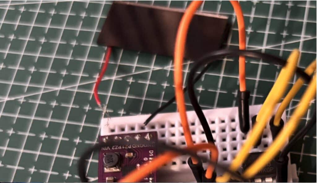
Now that we’ve established the connection with the IC, we can attach the PV cell and then add the battery or supercapacitor at Vout and GND. In our design, we configured the circuit for 3Vout, so a 3V supercapacitor can be added and start storing charge by harvesting ambient light.
Also Check: 10 innovative solar electronics projects you can build at home.
