


Moving past fabrication focus, India explores advanced packaging where stacking, integration, and materials innovation begin to shape next generation electronic systems
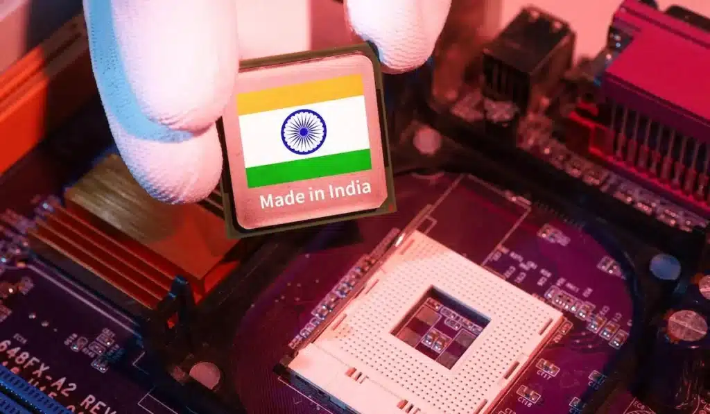
India’s semiconductor ecosystem is taking a step beyond conventional assembly with the introduction of advanced 3D chip packaging capabilities at Info Valley, Bhubaneswar. The new facility, led by 3D Glass Solutions, brings heterogeneous integration and embedded glass substrate technologies into the domestic manufacturing landscape, signalling a shift toward higher-value backend semiconductor processes.
At a technical level, 3D packaging enables multiple semiconductor dies to be stacked and interconnected within a single module, significantly improving bandwidth, reducing signal delay, and enhancing overall system efficiency. This approach is increasingly critical for modern computing architectures, particularly in AI accelerators and high performance systems where traditional planar designs struggle to meet performance and power demands.
A key differentiator in this facility is the use of glass substrates. Compared to conventional organic materials, glass offers improved thermal stability, lower signal loss, and higher interconnect density, making it well suited for high-frequency and high-reliability applications. This positions the technology for use across emerging domains such as 5G and 6G communications, automotive radar, defence electronics, and photonics.
From a system design perspective, the availability of advanced packaging within India could enable tighter integration between chip design and packaging, supporting the development of chiplet-based architectures. These modular designs allow different functional dies to be combined within a single package, optimizing performance, scalability, and cost across complex electronic systems.
The facility is expected to support a range of next generation applications, including artificial intelligence, high performance computing, and advanced communication infrastructure, where packaging is becoming as critical as the silicon itself.
Speaking at the event, Ashwini Vaishnaw, Minister IT, India said that the initiative would strengthen India’s semiconductor value chain, particularly in advanced technology segments, reinforcing the country’s push toward deeper integration in global electronics manufacturing.
Click here for the official announcement.