


Hybrid material integration enhances silicon photonics performance, enabling faster, energy-efficient data links for AI-driven data centres and next-generation optical interconnects.
Silicon photonics has gained a significant technological boost through the integration of new materials, potentially transforming high-speed data communication systems.
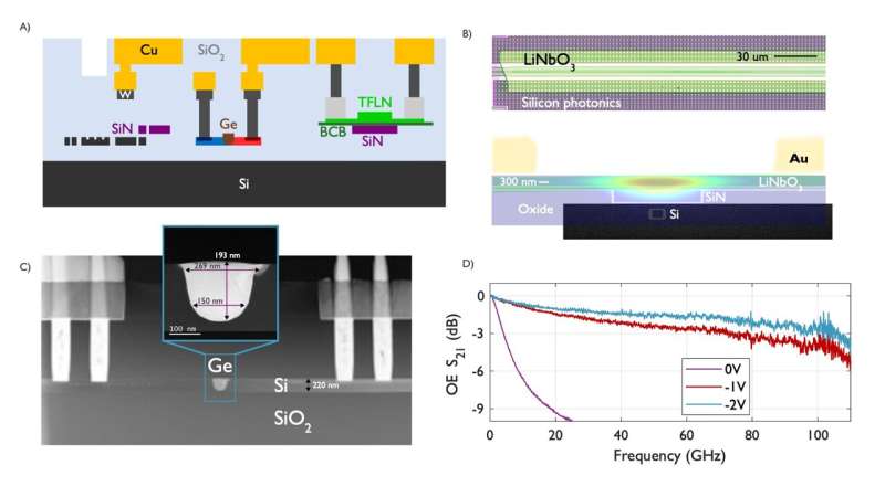
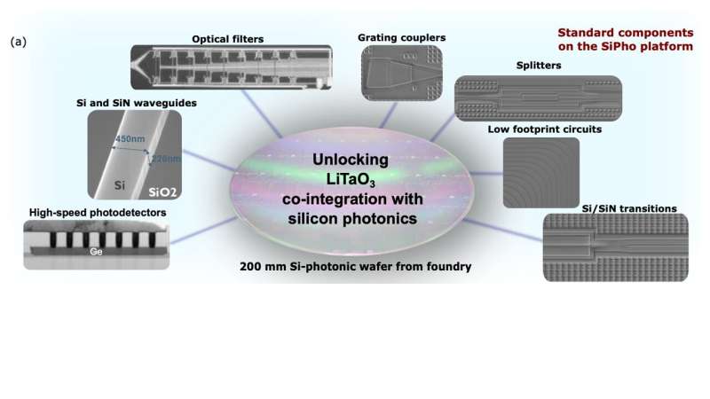
The advance centres on “heterogeneous integration,” in which non-silicon materials are integrated with silicon photonics platforms to improve performance. This approach enables the development of next-generation electro-optical components, including modulators and photodetectors, that are critical for high-speed optical links.
The timing is notable. Rapid growth in artificial intelligence and cloud computing is driving unprecedented volumes of data, increasing the need for faster and more energy-efficient interconnects within and between data centres. Current systems, typically operating around 200 Gb/s, are approaching their limits, pushing researchers to explore new architectures.
By incorporating advanced materials, silicon photonics devices can overcome inherent limitations of silicon alone—particularly in efficiently generating and detecting light. The result is improved bandwidth and reduced power consumption, both essential for scaling AI infrastructure.
Silicon photonics already plays a key role in modern communication systems by using light instead of electrical signals to transmit data, offering higher speeds and lower energy losses. However, expanding its capabilities has required innovations beyond traditional silicon-based designs.
The new integration strategy could enable short-reach and short-haul optical links capable of significantly higher data rates, addressing bottlenecks in data centre connectivity. This is particularly important as AI workloads demand faster communication between processors, memory, and storage systems.
Beyond performance gains, the approach is compatible with existing semiconductor manufacturing processes, which could ease large-scale adoption. Leveraging established fabrication infrastructure remains one of silicon photonics’ biggest advantages, allowing photonic and electronic components to coexist on the same chip.
While still evolving, the development highlights a broader shift toward hybrid photonic-electronic systems. As demand for high-bandwidth computing continues to rise, such innovations are expected to play a central role in next-generation networking and AI hardware ecosystems.