
Laser-written channels transform ordinary parchment into low-cost, eco-friendly electronic circuits, enabling disposable sensors and diagnostics without silicon while advancing paper-based electronics manufacturing.
Researchers at Binghamton University have demonstrated a new way to fabricate electronic circuits directly on everyday parchment paper, potentially reshaping low-cost electronics manufacturing.

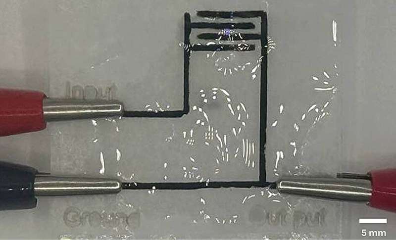
The technique uses a standard carbon dioxide laser to selectively modify the paper’s surface. By removing its silicone coating in precise patterns, the laser exposes cellulose fibers that readily absorb conductive inks. These treated pathways then guide water-based inks to form functional electronic components, including resistors, capacitors and interconnects.
This approach effectively converts common kitchen-grade parchment into a viable electronic substrate. The untreated regions remain water-resistant, acting as natural insulators, while laser-defined क्षेत्रों become conductive routes—allowing entire analog circuits to be created on a single sheet.
The development builds on more than a decade of work in “papertronics,” a field focused on replacing traditional materials like silicon and plastic with paper-based alternatives. Earlier efforts produced bio-batteries and wearable energy devices, but integrating complex circuitry has remained a challenge.
What sets this method apart is its simplicity and scalability. Unlike multi-step fabrication processes, the laser-writing technique enables direct patterning without additional chemical treatments or complex assembly. This could significantly reduce production costs while improving manufacturing speed.
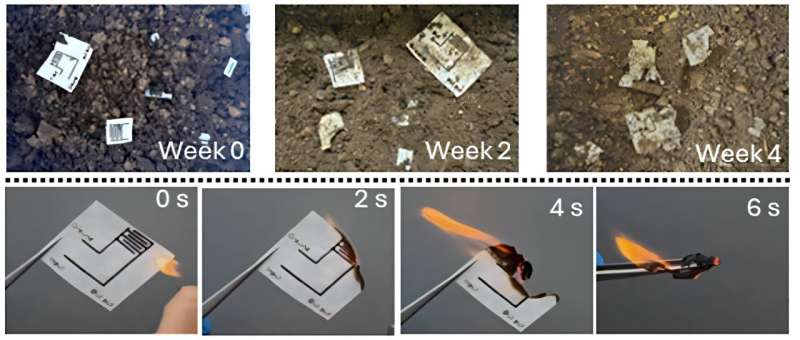
The implications are broad. Disposable electronics—such as smart food packaging, medical diagnostic strips, and environmental sensors—could be produced cheaply and sustainably. Paper-based circuits are also biodegradable, making them easier to dispose of compared to conventional electronic waste.
While still at a research stage, the technology signals a shift toward environmentally friendly electronics. By combining precision laser processing with widely available materials, it offers a pathway to scalable, low-impact electronic systems suited for short-term and single-use applications.
If commercialized, laser-patterned paper electronics could expand access to sensing and diagnostic technologies, particularly in cost-sensitive or resource-limited environments, while reducing reliance on traditional semiconductor fabrication.