India is developing its own processors from the ground up. Through its Vega chips, CDAC aims to deliver full control, AI capabilities, and custom designs, reshaping how industry, startups, and students work with silicon. Recently, Ashwini Kumar Sinha and Nidhi Agarwal from Electronics For You spoke with Krishnakumar Rao of CDAC about the architecture, challenges, and vision driving the development of an indigenous IP processor…
Q. Can you shed some light on what your centre is doing at CDAC?
A. CDAC is an autonomous organisation under the Ministry of Electronics and Information Technology, with 13 centres across India, including Guwahati, Mumbai, Pune, Bangalore, Hyderabad, Delhi, and Thiruvananthapuram. Across these centres, we have multiple groups working in areas such as high-performance computing, quantum computing, strategic electronics, software technologies, health informatics, cybersecurity, and education and training.

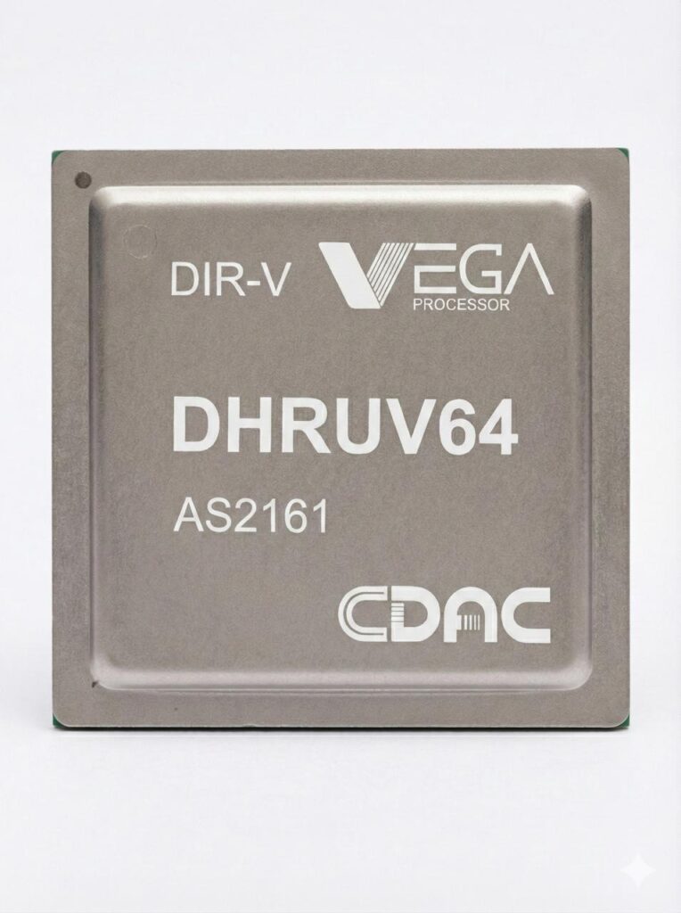
At our Thiruvananthapuram centre, as part of the Hardware Design Group, we are working on an indigenous processor development programme called DIR-V. This project is funded by our parent ministry, MeitY, and as part of it, we are developing a processor series under the brand VEGA.
Q. What was the inspiration behind starting an indigenous processor project in India?
A. Historically, all processors used in everyday products, such as washing machines, automobiles, mobile phones, televisions, PCs, and other daily-use electronics, have been imported. India did not have its own indigenous processor with full ownership and control. This led to initiatives in India to develop an indigenous processor with complete control over the design, source code, and all technical aspects, without dependence on foreign entities.
With this intent, discussions began at the government level, followed by a proposal submitted to the ministry. After receiving approval, formal project activities were initiated around 2018, although some groundwork, such as study and analysis- had already been underway.
Q. Which industries or applications are you targeting with this process?
A. The focus is on embedded applications across industrial, commercial, and strategic sectors. The processor series includes seven variants, all designed for embedded use, ranging from microcontroller-class devices to application-class processors. These can support a wide range of use cases, including IoT devices, drones, and more demanding tasks requiring high processing power.
Q. What makes the VEGA processor easy to change and use for different needs?
A. The VEGA processor is based on an open source RISC-V ISA, which was a key decision early in the project after discussions on the approach. This choice provides flexibility and allows the team to build a complete micro-architecture from scratch, without relying on external dependencies for features. The entire implementation is indigenous, covering the processor pipeline, cache design, and core interconnect. Because of this, there is full control from the ground up to the final implementation. This also creates a strong advantage when engaging with customers. Since we own the full processor design, we have started licensing it and can customise it based on specific application needs. There are no third-party constraints or external approvals required when making design changes, making the processor adaptable to different use cases.
Q. How much of the design is standard RISC-V, and how much is custom?
A. The processor is fully custom in terms of microarchitecture, but it is compliant with a specific flavour of the RISC-V instruction set architecture (ISA). That means different designers can build their own processors, each with its own microarchitecture, while still targeting the same RISC-V ISA standard. Functionally, the processors will execute the same instructions and produce the same results, assuming they are implemented correctly. From a functional perspective, they are equivalent. The difference lies in how each processor is implemented internally. So, while the ISA is standard (or a defined variant of it), the implementation, the microarchitecture, is entirely custom and specific to each design.
Q. What security features are built into VEGA processors to prevent hardware attacks?
A. The VEGA processor supports a secure boot feature. In the quad-core processor being developed, the secure boot feature is implemented, which integrates symmetric encryption standards such as HMAC and AES to ensure system integrity. Development is ongoing to add more advanced capabilities, including support for asymmetric algorithms. Security is treated as a continuous process, with each new variant improving on the previous one, making the overall system more robust and capable for end users.
Another key aspect of security comes from the processor’s indigenous design, which is transparent, with complete access to the source code and architecture. This ensures there are no hidden or unknown components in the system. Such transparency is important for strategic sectors like space, defence and atomic energy, which require full visibility into the design. The processor is built from the ground up with no black-box elements, making the entire system clear and verifiable.
Q. Can you explain the processing capabilities across your different processors, including core numbers, threading, multitasking, and architecture features?
A. We have a range of processors covering microcontrollers to application processors. At the microcontroller class, we have the 32-bit ET1031 and ET1037. Then we have a 32-bit application-class processor, the AT1051, capable of running Linux. Next, we have the AS1061, a 64-bit processor with a 6-stage pipeline. It supports compressed instructions, a single-precision and a double-precision FPU, and is highly customisable. If needed, we can configure it with or without the FPU.
The first three processors I mentioned, ET1031, AT1051 and AS1061, are all in-order, 32- or 64-bit processors. Moving to high-performance processors, we have 64-bit single-, dual-, and quad-core processors, which are out-of-order and more complex. They feature a 16-stage pipeline, integrated L1 and L2 caches, multiple execution pipelines, and are not currently multi-threaded but support out-of-order execution.
Q. Your processors are Linux compatible. Does that mean it can run Linux, and can it support AI workloads such as TensorFlow, PyTorch, or OpenCV on edge devices?
A. Out of all our processors, VEGA ET1031 and ET1037 do not support Linux. All our other processors, both 32-bit and 64-bit, are Linux-capable, and we have demonstrated them running Linux successfully. These processors can handle AI workloads on edge devices. For instance, the 32-bit processor supports TensorFlow Lite Micro, and the 64-bit processor supports TensorFlow Lite. They also work with frameworks like Edge Impulse and OpenCV. We have demonstrated applications such as person detection and object detection on these processors.
Q. Where do your VEGA processors and MCU series stand compared to platforms like Express chips, RP2040, or Raspberry Pi boards that can run a full Linux OS, in terms of computing power and positioning?
A. The current focus is not on directly competing with platforms like ST, RP2040, or Raspberry Pi. The initial goal was to develop indigenous IP and silicon. The first Aries Development board with THEJAS32 served as a feasibility test, and based on the interest generated, multiple variants were developed, with around 5000 boards deployed so far. Our main board, the Aries V3, was made pin-compatible with the Arduino UNO to ease adoption, allowing users to run existing Arduino shields and code directly. An Arduino plugin library was also developed so programs could compile and run on the VEGA-based board without changes, helping to build a supportive ecosystem.
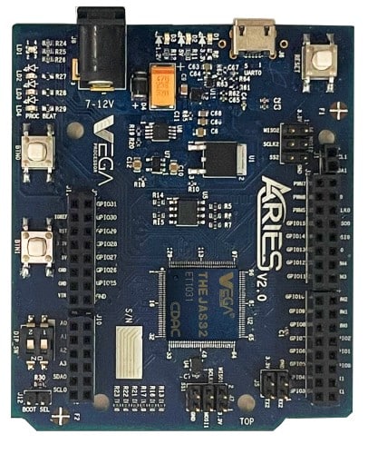
The board runs at 100MHz on a 32-bit architecture, offering better computing and specifications than a typical Arduino. However, it was not intended as a replacement but to raise awareness of VEGA, which was largely unknown even in academia 4–5 years ago. Adoption has since grown, with academic institutions using the boards for learning and research. Academic and industrial adoption are progressing in parallel, reinforcing the ecosystem around VEGA.
Q. Does your processor act as a base that allows engineers to design their own applications and add custom elements as needed?
A. The processor serves as a base; you can add your secret IP or other custom modules and build the final product. We support this for FPGA-based solutions as well. For certain strategic applications with low volume requirements, we deploy the processor on FPGA boards. In these cases, the board integrates our processor, additional in-house IP and sometimes IP provided by the customer, creating a fully indigenous solution tailored to their needs.
Even if the customer only requires a few boards rather than thousands, we can provide a complete solution that meets their specifications. Essentially, we provide a reference SoC design that acts as a base for engineers to develop custom applications. Whether it is a system-on-chip or an FPGA-based design, we supply the necessary IP, enabling engineers to integrate their own accelerators or modules with the generic processor. There are no restrictions; we actively support customers in building their custom applications on top of our platform.
Q. What range of peripherals does your processor and MCU support, and do you provide customisation for specific user needs?
A. We support a wide range of peripherals, including SPI, Quad SPI, USB 2.0, 10/100 Ethernet, and Gigabit Ethernet, most of which are homegrown IPs developed and extensively tested. Many of these IPs are already deployed across various industry applications, demonstrating reliability and versatility.
At the same time, our processor uses a standard interface that allows seamless integration of third-party IPs. For example, while we don’t provide a CAN interface, users can easily plug in third-party CAN IP to build their SoCs. In our test chips, we have already integrated third-party IPs where needed, such as an external PLL or a DDR controller and PHY, without any compatibility issues. The system supports plug-and-play integration and allows customisation for user-specific peripherals.
Q. How do your processors and MCU series handle memory, and can engineers extend it if needed?
A. There is no strict restriction on the memory you can connect. Typically, in our SoC designs, partners provide some internal SRAM and then add external DRAM using a DRAM controller. DDR memory is commonly used, but any combination is possible; there is no limitation. The processor also supports Level 1 and Level 2 caches, which can be customised in size based on the application. On-chip memory can be added without restriction, depending on design needs. For external memory, we can interface with any third-party DDR controller or on-board DDR memory. SDRAM is also supported; in one of our designs, we integrated an SDRAM controller on the chip and connected SDRAM on the board. Overall, memory extension and configuration are flexible and fully dependent on the design implementation.
Q. How does the processor support other functions like ADC, DAC, I2S communications for microphone or audio processing, and can custom integrations be handled?
A. We don’t have an in-house ADC IP, but interfacing with any standard ADC is supported.
The processor supports standard interfaces, and the interface can also be modified to add a bridge or include glue logic as needed. Each user often has unique requirements, like a smaller cache, interface changes, or a specific accelerator, so supporting custom changes is essential. Our goal is to make the processor flexible and usable across different industrial applications by enabling any integration that engineers require.
Q. How does the camera interface work, USB, CSI, or some other internal camera support? And do you have an ASIC that supports cameras and Wi-Fi?
A. On the FPGA, we can connect various interfaces, including cameras, and have demonstrated that it works. Technically, this isn’t an issue, but we don’t currently have an ASIC that integrates cameras, CSI, or Wi-Fi. Applications are very diverse, and a processor can be used to develop SoCs for different applications, making a one-size-fits-all solution impractical. Instead, we create scenarios to validate the processor’s capabilities, testing it on an FPGA with various interfaces to demonstrate it can handle a range of functions and their derivatives.
Q. What software tools, compilers, and programming environments are supported for the VEGA processor, and do developers need separate modules for IoT connectivity like Wi-Fi or Bluetooth?
A. The VEGA processor is compatible with the open source compiler toolchain provided by RISC-V. This means anyone can design, compile, and run programs on VEGA using standard open source tools. Developers can also use the Arduino IDE, which is widely used in academia. The underlying GNU toolchain operates in the background, and a board support package has been created to enable compatibility with Arduino. While the toolchain is fully open and not customised at present, future additions like custom instructions may require compiler modifications, though there has been no need for that yet. On the hardware side, Vega chips do not currently integrate IoT connectivity such as Wi-Fi or Bluetooth. To enable these features, a separate external module must be added.
Q. Are the VEGA boards meant only for prototyping, or can they also be used in real products? How are they being used across academia and industry?
A. The VEGA boards were created for development and prototyping, starting with a 32-bit microcontroller-class chip. Initially, only engineering samples were shared with a few academic institutions and start-ups, which sparked interest and requests for wider access. This led to small-scale prototyping expanding into multiple board versions, beginning with V2 and later evolving into IoT-focused boards and V3 variants, shaped by feedback from both academia and industry. While some users have integrated these boards into products, the primary goal has been to raise awareness and adoption of the RISC-V ecosystem.
To address this, boards were distributed to academic institutions, and hands-on workshops were introduced in which design engineers guide BTech and MTech students in building small applications on an indigenous processor. Over the past three to three-and-a-half years, around 120 workshops have been conducted nationwide. The focus remains on RISC-V, with VEGA serving as a learning platform. On the industry side, a few startups have adopted the 32-bit chip, designing their own boards, while a training-focused company developed a VEGA-based board and now uses it in their programs.
Q. Do you have a community or support system for developers, students, or startups using your development boards or VEGA chips?
A. Yes, we provide multiple support channels. There is a YouTube channel, a discussion forum, and a blog to help developers. We also have a direct mobile number and email ID for one-on-one queries. For academic institutions, we engage extensively, conducting around 2–3 workshops per month. These workshops include half-day lectures and half-day practical sessions where participants work with VEGA boards, sensors, and actuators. Many institutions have also purchased ARIES boards for their labs. We provide them support through calls, emails, or online meetings. We also provide individualised support to design engineers and startups seeking to develop their products using VEGA chips.
Q. Do you provide sourcing or R&D support for startups and academic institutions?
A. Yes. Several startups have designed their own boards based on the THEJAS 32 using our reference designs as a starting point. They can add, remove, or modify features, including the form factor, according to their ideas. Typically, they create the schematic and share it with us for review. We provide guidance through online meetings, advice on necessary changes, and support them throughout board design and testing.
For IP development, we provide VEGA-based FPGA designs to industry and academia, enabling them to implement and test them. We also host hackathons and challenges where users can integrate their own IP into VEGA-based designs. Over the past two years, we’ve collaborated with the annual Design & Verification Conference (DVCon) on their design contest, supporting it with VEGA processor-based designs.
Q. What were the biggest challenges in designing a high-performance RISC-V SoC from scratch in India?
A. One of the biggest challenges was securing the right talent. Hiring experienced processor designers is difficult, as specialised expertise is limited in India. We built on prior experience from an earlier processor based on a different ISA, while training fresh graduates and also collaborating with IITs to form the team. This issue is not limited to government projects; very few companies in India work deeply in this space. Many successful startups are led by Indian-origin professionals in Silicon Valley with 20–30 years of experience at firms like Apple, Google, or Intel, experience that is hard to find locally.
Fabrication was another major hurdle, since we had to rely mostly on external foundries. The first chip was fabricated at Silterra in Malaysia, the second at SCL Chandigarh (180nm), and the third at TSMC (28nm) in Taiwan. Initial tape-outs were test or shuttle runs to validate designs. As a smaller player, securing slots with major foreign foundries was difficult because foundries prioritise large-volume customers, and procurement and coordination with foreign entities were challenging. Post-COVID supply constraints and memory shortages made access even harder. The situation is, however, improving, with initiatives like the India Semiconductor Mission and upcoming domestic foundries by Tata, which should make chip design and manufacturing in India easier.
Q. What was the most challenging technical aspect while designing the processor—pipeline, cache, interconnect, or something else?
A. Designing and architecting the processor is definitely a challenge, but the bigger challenge is verification. Unlike fixed-function designs or application-specific modules, where the use case is known and testing can be focused, processor design is general-purpose. It can run any application, used by different users in different scenarios. That makes verification much harder. You have to ensure that everything works correctly across all possible use cases, not just a specific one. So while design is complex, verification is equally, if not more, challenging because it requires ensuring the processor is functionally correct and free of bugs under a wide range of conditions.
Q. How did you ensure verification completeness for such a complex SoC, and reach confidence that it is fully verified?
A. Verification followed a layered approach. It began at the module level, covering components like the pipeline and cache. After module-level verification, the modules were integrated to form the processor, where testing continued at the processor level. Initial simulations were run, followed by execution on an emulation platform. Once sufficient confidence was achieved, the design was implemented on an FPGA using a minimalistic SoC built around the processor. This SoC included basic infrastructure, an Ethernet interface for connectivity, a UART for terminal access, an SDRAM or DRAM interface for instructions and data, and program memory for verification.
Extensive FPGA testing was conducted using standard routines, publicly available tests, and third-party EDA vendor tools that generate a wide range of test routines. These tools supported long regression runs with self-checking mechanisms to detect failures. Once initial tests passed, more exhaustive verification was performed, covering different instruction classes, instruction types, combinations, and randomised scenarios. This iterative, multi-pronged process ensured thorough verification and high confidence in the processor design.
Q. How mature was the RISC-V ecosystem when you started, and how has it evolved today?
A. When we began, the RISC-V ecosystem was very small, with mainly one known company, SiFive and a few others working in the space. Since then, it has grown substantially, with many startups and multinational companies joining the ecosystem. The RISC-V International community now counts around 4000–5000 members. Its open source nature has fueled this growth, and we contribute to it as well. In India, adoption has increased, supported by government initiatives, localisation efforts, and interest from public sector units and strategic labs exploring this ISA.
Despite this progress, RISC-V is still less mature than ARM. However, the ecosystem shows clear momentum, with deeper engagement across industries and geographies. When we began, there was uncertainty about widespread adoption, but today, many players actively work with RISC-V. The ecosystem continues to evolve, gaining both speed and depth as it moves steadily forward.
Q. Can RISC-V help India build a full semiconductor stack, and what does that stack include?
A. Yes, RISC-V can help India build a full semiconductor stack, covering the entire value chain from chip design and IP to fabrication, testing, and product deployment. Today, it acts as a catalyst, supported by government initiatives like the design-linked incentive (DLI) scheme, which provides access to EDA tools, financial support for manpower, and subsidised IP. Many companies under the scheme have already started adopting RISC-V for the chips and devices they are developing. The key advantage is that RISC-V removes a major barrier to entry: unlike proprietary architectures, it eliminates upfront licensing fees and royalties, allowing Indian companies to design their own processors and SoCs more freely. This shift is already visible, with several Indian firms designing RISC-V-based processors and SoCs, though many are currently fabricated outside India.
Looking ahead in the next 2–3 years, large-scale impact may remain limited, but over 5–10 years, significant developments are expected. Within 4–5 years, a more complete stack could emerge, including chips designed in India using largely indigenous IP, fabricated in domestic foundries such as Tata’s upcoming facilities, followed by testing, reference design development, and production. Since Indian designs are already in development, these domestic foundries will have a ready customer base once operational. Over time, this ecosystem, driven by RISC-V and government support, can enable India to establish a self-reliant, end-to-end semiconductor industry.
Q. What challenges did you face while working with the RISC-V framework? Were there any limitations?
A. There were no major architectural limitations. In the early stages, some specifications were still evolving since it is an open ISA. Instruction-set extensions such as integer, multiply, atomic, single-precision, and double-precision were defined first. But vector support was not available initially, while compressed instructions existed earlier. As the ISA matured and specifications were finalised and published, development aligned with those updates, so the work progressed in sync with the evolving standard.
Q. What gaps do you still see in the ecosystem, particularly regarding government support or the use of RISC-V for making processors?
A. From the government side, we don’t see major gaps. The government is already strongly supporting these activities and promoting indigenous technology, which is becoming increasingly important amid a changing geopolitical landscape. With backing from the parent ministry, India is actively driving initiatives and supporting the adoption of such technologies. On the government front, things are progressing well.
The gaps are mainly on the technical and ecosystem side. RISC-V has existed for only 10–12 years, while ARM and similar technologies have been around for 30–40 years, so the ecosystem is still growing. Today, third-party compiler toolchains and open source tools are available, and for debugging, we rely on standard SDK capabilities alongside third-party debuggers and adapters. Companies that support ARM are increasingly offering RISC-V tools as the market grows. While it will take time for RISC-V to match ARM’s ecosystem maturity, private investment, government support, and emerging robust tools give us confidence it will reach that level.
Q. Are there any future plans to develop a chip with integrated radio bands and IoT connectivity? How challenging is it to design such a chip?
A. Currently, we don’t have any immediate plans to build a system-on-chip with integrated Wi-Fi or other wireless features. Integrating radio bands and IoT is challenging because, to my knowledge, the IP required isn’t available domestically; we would need to license it from outside India and then integrate it. That work requires careful design and support. Right now, we don’t have plans to pursue it ourselves, but if a customer requests it, we are happy to support them. In fact, one of our customers is already working on such an integration themselves, and while we won’t do it directly, we are very open to helping others who need it.
Q. What improvements are planned for the next version of your processors?
A. The improvements are ongoing and focus on three main areas. First, we collaborate closely with industry partners who use our processors and often have specific requirements, such as changes to the processor interface, cache memory, or replacement policies. We adapt the design to meet these customer-specific needs. Second, we are adding new features, particularly in security, where we see significant potential for enhancement.
Third, we have initiated preliminary work on a server-class processor to build an indigenous solution for enterprise applications. In summary, our efforts focus on enhancing core features such as security, customising processor elements based on customer requests, and developing the next-generation server-class processor, with all activities progressing concurrently.