


Aims to simplify large-panel semiconductor packaging, improve manufacturing efficiency, and support finer circuitry and multi-layer structures required for AI-driven chip designs.
A newly developed photosensitive film technology by Asahi Kasei could address growing manufacturing challenges in advanced semiconductor packaging as the industry shifts toward larger formats, higher circuit density and increasingly complex chip architectures.
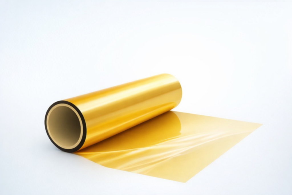
The material combines characteristics traditionally found in liquid photosensitive polyimide (PSPI) and dry film photoresist technologies, creating a film-based solution intended for panel-level semiconductor packaging processes. The approach is designed to improve production efficiency while supporting finer circuitry and more complex package structures increasingly required in AI and high-performance computing applications.
Panel-level packaging is gaining industry attention because it allows manufacturers to process larger square panels rather than smaller circular wafers. The transition is expected to improve manufacturing throughput and yield while lowering production costs. However, the shift also introduces challenges related to material uniformity, process control and multi-layer integration.
The new film aims to tackle these issues through lamination-based application methods that enable more uniform coating across larger surfaces. This may help reduce processing complexity and support scalable production of advanced semiconductor packages.
The key features are:
- Combines liquid PSPI and dry film photoresist properties
- Supports panel-level lamination processing
- Designed for fine circuit pattern formation
- Enables higher insulating layer counts
- Compatible with 3D packaging copper pillar structures
The material is being evaluated for use in redistribution layers and insulating layers in package substrates. Redistribution layers are critical in semiconductor packaging because they create electrical pathways between chips and external connections. As semiconductor packages continue evolving toward denser and more three-dimensional structures, insulation materials are also required to support a higher number of stacked layers.
The technology is also being developed alongside fine-patterning and copper pillar formation processes. Combined solutions are expected to support sub-micron circuit structures and high-aspect-ratio copper pillars needed in advanced three-dimensional packaging architectures.
Demand for such materials continues to rise as AI infrastructure expands and chip manufacturers seek ways to integrate more functionality into smaller footprints. Larger interposers, increased wiring density and additional package layers are placing greater performance requirements on packaging materials.
As semiconductor packaging moves from wafer-level approaches toward larger panel-based and three-dimensional designs, material innovation is becoming an increasingly important factor in maintaining manufacturing efficiency while meeting next-generation performance requirements.
Click here for the original announcement.
