


What happens to stored energy after a system shuts down? This design shows a way to discharge it only when needed.
High-voltage DC-link capacitors are widely used in electric vehicles, industrial motor drives, renewable energy systems, and power converters. While these capacitors are essential for energy storage and power conditioning, they also present a safety challenge. Even after a system is powered down, the capacitor can retain a hazardous voltage for an extended period, creating a risk of electrical shock during maintenance or servicing.
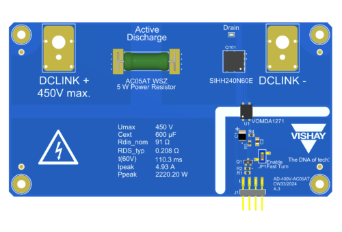
A reference design from Vishay addresses this challenge with an active discharge circuit capable of safely discharging a DC-link capacitor while minimizing power losses during normal operation.

Traditionally, designers have relied on bleed resistors connected permanently across the DC-link capacitor. Although simple, this approach continuously dissipates energy whenever the system is operating. In applications where efficiency is critical, such as EV traction inverters and industrial drives, this constant power loss becomes undesirable.
The active discharge approach solves this problem by activating the discharge path only when required. Instead of continuously drawing power, the circuit remains inactive during normal operation and initiates discharge only after a shutdown event or safety trigger.
The reference design supports DC-link voltages from 25 V to 450 V and is designed around a Super Junction (SJ) silicon MOSFET acting as the discharge switch. The MOSFET is controlled by a photovoltaic gate driver, which provides galvanic isolation while eliminating the need for a dedicated isolated power supply. This simplifies the overall design and reduces component count.
One of the notable aspects of the design is its ability to discharge a 600 µF capacitor from 450 V to 60 V in less than two seconds. This enables compliance with safety requirements that specify maximum discharge times for exposed high-voltage systems.
The discharge energy is dissipated through a pulse-proof resistor connected in series with the MOSFET. Since discharge events occur only occasionally, the resistor experiences short-duration energy pulses rather than continuous power dissipation. Designers can select different resistor technologies depending on application requirements. The reference design evaluates several options, including wirewound, thick-film, and carbon-film resistor types, allowing optimization for pulse handling capability, thermal performance, and board space.
The photovoltaic gate driver plays a key role in the circuit. When a control signal is applied, the driver generates the gate voltage required to turn on the MOSFET. Once activated, the MOSFET provides a controlled discharge path for the stored capacitor energy. Because the gate driver is optically isolated, the low-voltage control circuitry remains separated from the high-voltage DC bus, improving system safety.
For design engineers, the reference design offers a practical solution for meeting safety standards without sacrificing efficiency. The architecture is scalable and can be adapted to different DC-link capacitances, discharge times, and voltage levels by selecting appropriate MOSFET and resistor values.
Vishay has tested this reference design. It comes with a bill of materials (BOM), schematics, assembly drawing, printed circuit board (PCB) layout, and more. The company’s website has additional data about the reference design. To read more about this reference design, click here.
