


A newly developed semiconductor device performs multiple computing tasks simultaneously, reducing component requirements by 75% and boosting processing speeds fourfold, opening new possibilities for compact AI-enabled electronics.
A semiconductor technology could reshape the design of next-generation electronic devices by enabling a single-chip component to perform multiple computing functions simultaneously, significantly reducing hardware complexity while accelerating performance.

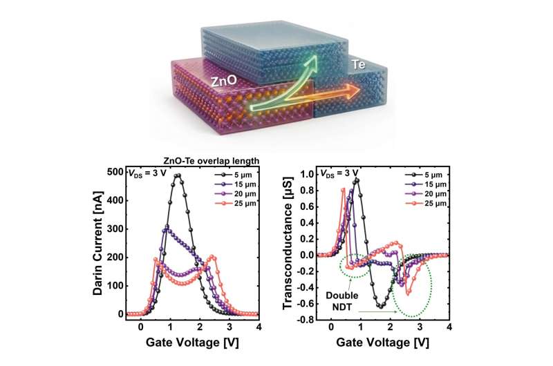
Researchers at Pohang University of Science and Technology have developed a new semiconductor device that cuts the number of required components by 75% and delivers processing speeds up to four times faster than conventional approaches. The innovation addresses a growing challenge facing the electronics industry: fitting increasingly powerful computing capabilities into smaller devices without driving up power consumption or design complexity.
As artificial intelligence workloads expand from cloud servers to smartphones, wearables and edge devices, chipmakers are under pressure to process larger volumes of data within tight space and energy constraints. Traditional semiconductor architectures often rely on multiple dedicated components to handle different computational tasks, creating bottlenecks in performance, size and efficiency.
The newly developed device takes a different approach by integrating several functions into a single semiconductor element. Instead of assigning separate hardware blocks to individual operations, the technology allows one device to switch between and execute multiple tasks, effectively introducing a “multi-tasking” capability at the hardware level. This consolidation reduces circuit complexity while improving data-processing throughput.
According to the researchers, the architecture could help electronics manufacturers build smaller and more capable systems without increasing chip area. The reduction in component count also has the potential to lower manufacturing costs and simplify circuit design, making advanced computing more practical for compact consumer and industrial devices.
The development arrives at a time when semiconductor innovation is increasingly focused on efficiency rather than simple transistor scaling. With AI applications demanding greater computational density, technologies that combine higher performance with lower hardware overhead are becoming critical to future electronics roadmaps.
If successfully commercialized, the new semiconductor design could find applications in edge AI systems, wearable electronics, smart sensors and other devices where space, power efficiency and processing speed are key requirements. The advance signals a shift toward more versatile chip architectures capable of handling diverse workloads within a single compact platform.
