


New agentic EDA capability is positioned to execute design and verification tasks with minimal human intervention, aiming to compress simulation-heavy workflows and speed time-to-silicon.
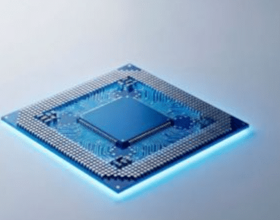
A new autonomous “virtual engineer” for semiconductor development has been introduced by Cadence, with the vendor positioning it as the industry’s first Level‑5 agentic AI system capable of performing substantial chip design and verification work without continuous human supervision. The launch targets one of the most time‑consuming bottlenecks in modern silicon programs: running, analyzing, and iterating millions of verification and simulation tasks across increasingly complex SoCs.

The system extends an existing AI‑assisted chip design platform into a fully autonomous mode. Rather than acting only as a copilot, the software is designed to plan workflows, invoke EDA tools, launch dynamic simulations, evaluate results, and continue optimization loops inside a governed environment. According to the announcement, the stack combines electronic design automation software, large language models, and a secure runtime intended for enterprise deployment.
Main tech features
- Level‑5 autonomous workflow orchestration for chip design and verification.
- Agentic AI framework that can launch, monitor, and iterate dynamic simulations automatically.
- Integration with signoff‑class EDA engines inside governed workflows.
- GPU‑accelerated AI runtime and large‑model stack for scalable execution.
- Designed for enterprise security, auditability, and controlled automation.
The most immediate value proposition is verification acceleration. The vendor said large engineering organizations already run millions of tests and consume massive compute resources during chip validation, and that autonomous orchestration can dramatically reduce turnaround time for RTL verification and related debug cycles. Industry observers have previously noted that verification often dominates semiconductor schedules, making automation gains especially attractive for AI, data center, automotive, and advanced compute projects.
Under the hood, the platform is built around an agentic framework that coordinates simulation, verification, and analysis tasks across existing signoff‑class tools, while GPU infrastructure and AI models provide the reasoning and execution layer. The company also emphasized security controls, auditability, and governed workflows as requirements for deploying autonomous agents in production chip programs.
The broader significance is that EDA vendors are moving beyond AI assistants toward workflow autonomy. Instead of generating scripts or answering questions, the new class of tools is intended to execute multi‑step engineering tasks end‑to‑end, with human engineers shifting toward supervision, constraints, and signoff decisions. Early access to the autonomous capabilities is planned before broader availability, signaling that practical deployment will likely begin with selected customers and high‑compute verification use cases.
Click here for the original announcement.