


Can an electronic device identify spoiled food and hidden allergens before people can? An ML based system is making it possible.
Researchers at the University of California, Berkeley have developed an electronic nose capable of detecting gases released by spoiled food and identifying common food allergens with greater sensitivity than the human sense of smell. Described as a proof of concept, the device combines an array of miniature gas sensors with machine learning to recognise the unique chemical signatures of different foods, offering a potential tool for improving food safety and reducing waste in homes and commercial settings.
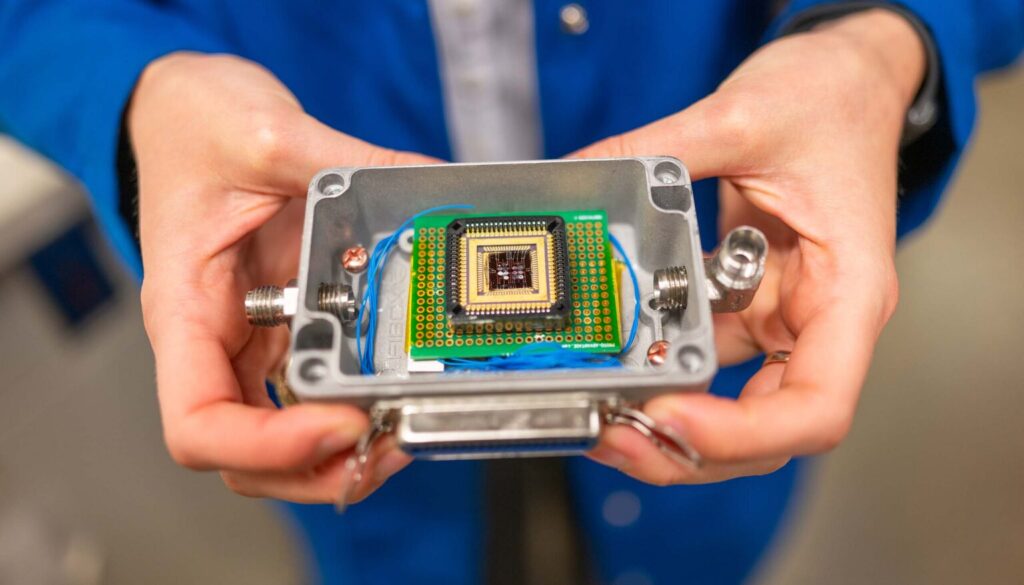
The sensing chip contains 16 gas sensors, each coated with a different sensing material that responds to specific combinations of airborne compounds. Instead of identifying a single gas, the system analyses the collective response of all sensors to create a distinctive chemical fingerprint. Researchers trained a machine learning model using gases released from fruits, nuts, milk, eggs, and raw chicken at different stages of freshness. During testing, the system successfully distinguished fresh food from samples left at room temperature for up to 48 hours. It was also sensitive enough to detect as little as 0.05 grams of walnut, demonstrating its potential for allergen detection.
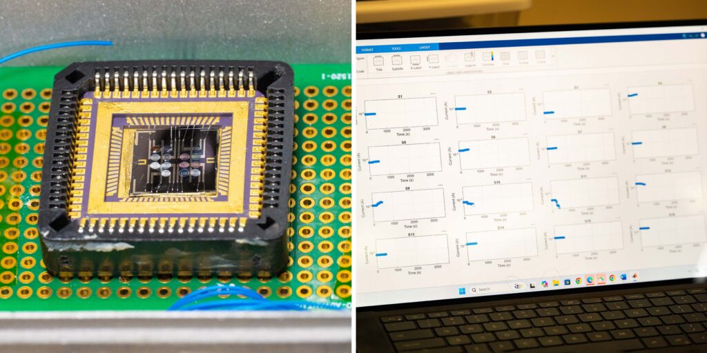
One of the key engineering advances lies in the use of carbon nanotubes instead of conventional metal oxide materials. Carbon nanotubes operate at room temperature, allowing the researchers to incorporate a wider range of sensing materials, including temperature sensitive polymers. This also simplified manufacturing by enabling all sensing films to be deposited in a single fabrication step. The approach overcomes a major challenge that has limited the practical development of electronic noses for decades.

Lead author Carla Bassil, a Ph.D. student in electrical engineering and computer sciences at Berkeley, says, “The truly scalable aspect of my electronic nose is that we can use all these different types of sensing materials while depositing them all in a single step,” highlighting the device’s simplified fabrication process, which enables multiple sensing materials to be integrated onto a single chip without complex manufacturing techniques.
