




A new layered acoustic chip architecture overcomes long-standing power limitations in RF devices, enabling cooler operation, higher power handling and improved reliability for future 6G, satellite and quantum systems.
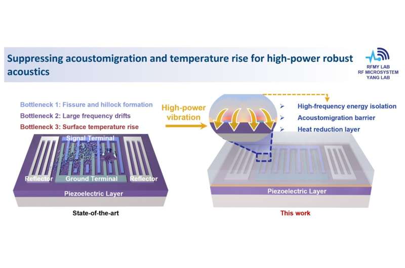
Researchers at the Hong Kong University of Science and Technology (HKUST) have developed a new acoustic chip architecture that can withstand more than 12 times higher power than conventional designs while significantly reducing heat generation. The breakthrough could remove one of the biggest limitations in radio-frequency (RF) acoustic devices, enabling more robust hardware for 6G networks, direct-to-cell satellite communication, quantum computing and compact power electronics.
Acoustic wave devices are widely used in smartphones and wireless base stations to filter RF signals. They convert electrical signals into high-frequency sound waves, allowing compact filtering of gigahertz-frequency signals. Despite their widespread use, these chips have traditionally been limited to low-power operation because excessive heat and mechanical stress cause metal migration, frequency drift and cracks in the piezoelectric layer, ultimately leading to device failure.
To address this challenge, the HKUST team developed a Layered Acoustic Wave (LAW) architecture that redesigns the top surface of the device rather than relying on expensive high-thermal-conductivity substrates beneath it. The approach places a silicon dioxide isolation layer and a thick amorphous silicon layer above the lithium niobate acoustic device. This layered structure redistributes mechanical stress, improves heat dissipation and compensates for thermal expansion without allowing acoustic energy to escape.
Laboratory testing showed the new architecture reduced steady-state temperature rise by about 70% while achieving a record power-density threshold of 36.4 W/mm². The structure also lowered damping losses by around 30% and increased operating frequency by approximately 25% without requiring complex fabrication techniques. Failure analysis revealed that conventional thin-film surface acoustic wave devices exhibited electrode migration and material cracking under high power, whereas LAW devices remained intact under substantially higher operating loads.
Unlike previous approaches that primarily focused on improving substrate materials, the LAW design tackles the root causes of failure by engineering the device boundary where heat and stress originate. Because the concept is based on structural design rather than a specific material system, it can be adapted to a broad range of acoustic devices that use interdigital transducers.
Beyond RF filters for smartphones and wireless infrastructure, the technology could support high-power acoustic components for direct-to-cell satellite links, cryogenic quantum acoustic circuits, on-chip acousto-optic and microfluidic systems, and compact nonmagnetic power-conversion modules, expanding the role of acoustic chips well beyond signal filtering.


