The next efficiency gain in electronics assembly may not come from faster machines, but from controlling what happens at every stage of the line.
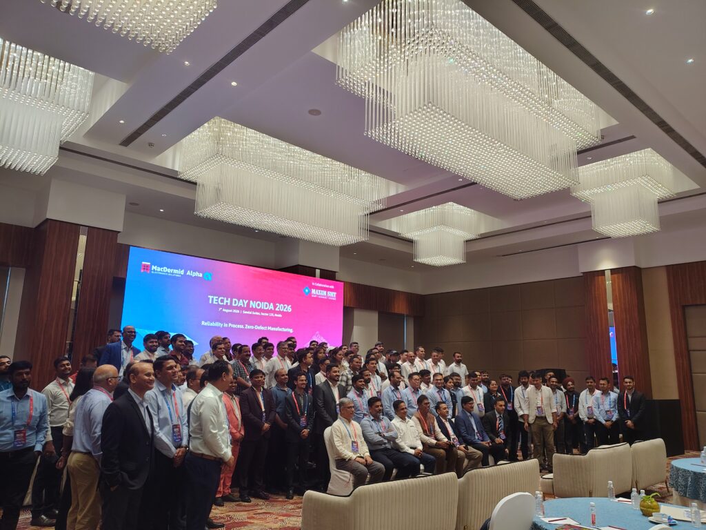
As electronic assemblies become smaller, denser, and more application-specific, manufacturing efficiency can no longer be measured by production speed alone. Material choices influence cost, printing affects solder quality, protective materials determine environmental durability, and testing establishes whether the finished assembly is ready to leave the factory.
The shift towards tighter control across these stages is becoming increasingly important for electronics manufacturers looking to improve production consistency while managing cost and reliability. Four areas in particular illustrate how this approach is evolving: solder materials, stencil printing, polymer protection, and production testing.
Soldering: Cutting Material Cost Without Losing Reliability
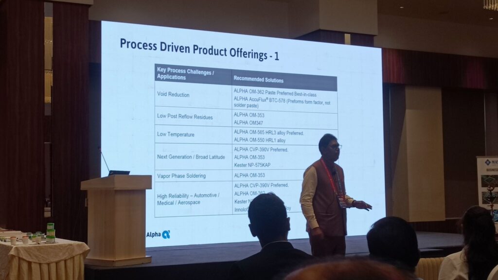
Silver remains an important cost consideration in lead-free soldering. SAC305, a widely used alloy for electronics assembly, contains approximately 3 per cent silver, creating an opportunity to reduce material cost by changing the alloy composition.
A silver-free solder alloy positioned as an alternative to SAC305 removes the silver while retaining a tin-based soldering system and is intended to work with existing assembly processes.
“The only thing is we are removing 3 per cent silver out of the box,” said Richard Puthota, senior director, MacDermid Alpha, while discussing the formulation and its cost implications. Thermal cycling, drop, and vibration testing have also been used to assess the alloy.
The approach, however, is application-dependent. Puthota noted that the material should not be considered for applications requiring operation beyond approximately 100°C without further evaluation. Internet of things (IoT) devices, lighting, routers, and other electronics operating within the relevant range represent potential applications.
For electronics manufacturing services (EMS) companies and original equipment manufacturers (OEMs), the calculation therefore extends beyond the price of solder. Any material saving has to be weighed against qualification requirements, reliability expectations, and the possibility of additional process or testing costs.
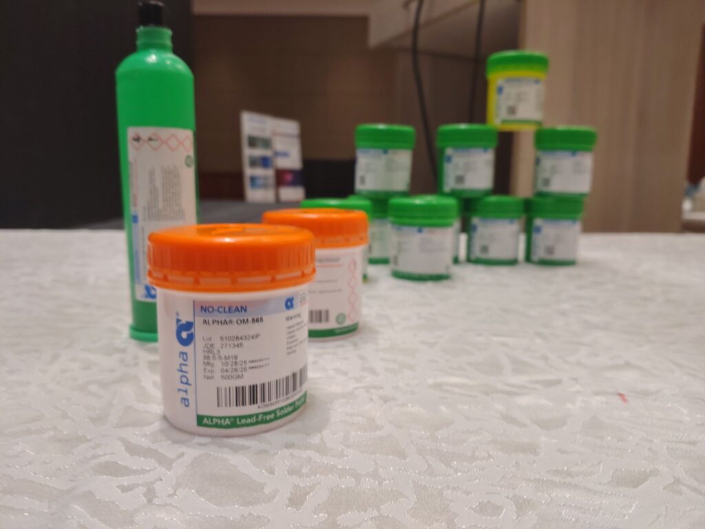
Stencil Printing: Improving Solder-Paste Transfer
Once the solder material is selected, the next challenge is getting the right amount of paste onto the right locations.
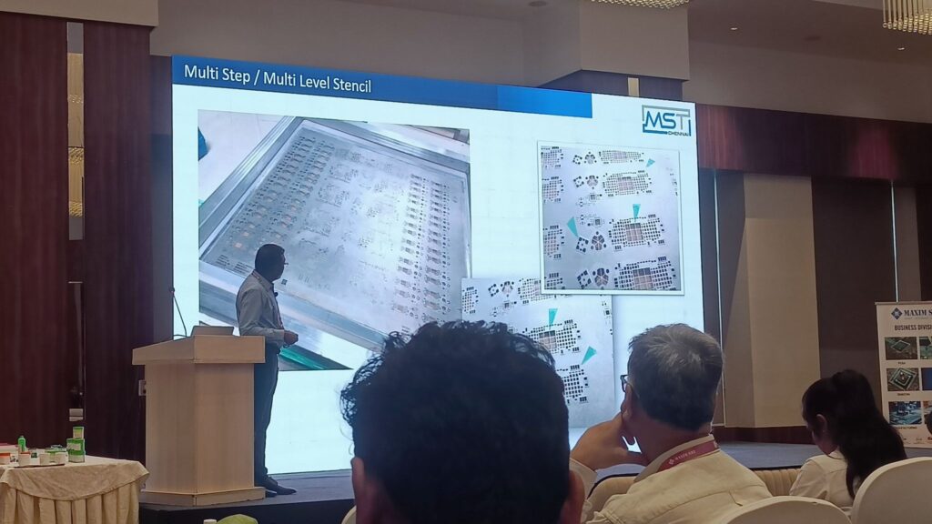
Material efficiency also depends on how consistently solder paste is transferred to the board. As component geometries become smaller, controlling paste release through increasingly fine stencil apertures becomes more important.
A chemical vapour deposition (CVD)-based nano-coating for surface mount technology (SMT) stencils addresses this stage by depositing a hydrophobic coating inside a vacuum chamber, including along the stencil aperture walls. The surface is intended to reduce friction during paste release and improve transfer consistency, particularly around smaller apertures, while potentially extending intervals between under-stencil cleaning.
The technical discussion, however, also raised a practical question around quality verification. Contact-angle measurements and laboratory analysis can indicate coating characteristics, but verifying coating thickness across individual apertures is more demanding. Detailed measurements require techniques such as scanning electron microscopy and are generally performed through sampling.
That places greater emphasis on the output of the printing process itself. Consistent solder-paste transfer remains the practical measure of whether a stencil treatment is delivering the intended production benefit.
Sakthivel Padmanapan, general manager, MST Chennai, demonstrated the CVD-based stencil-coating approach.
Extending Reliability Beyond Reflow
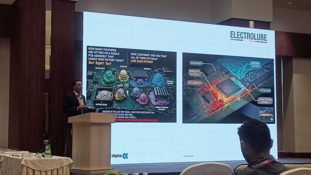
A soldered assembly can still fail when exposed to moisture, temperature variation, chemicals, dust, or electrical bias. Protective polymers therefore form another layer of manufacturing control, particularly for products expected to operate in demanding environments.
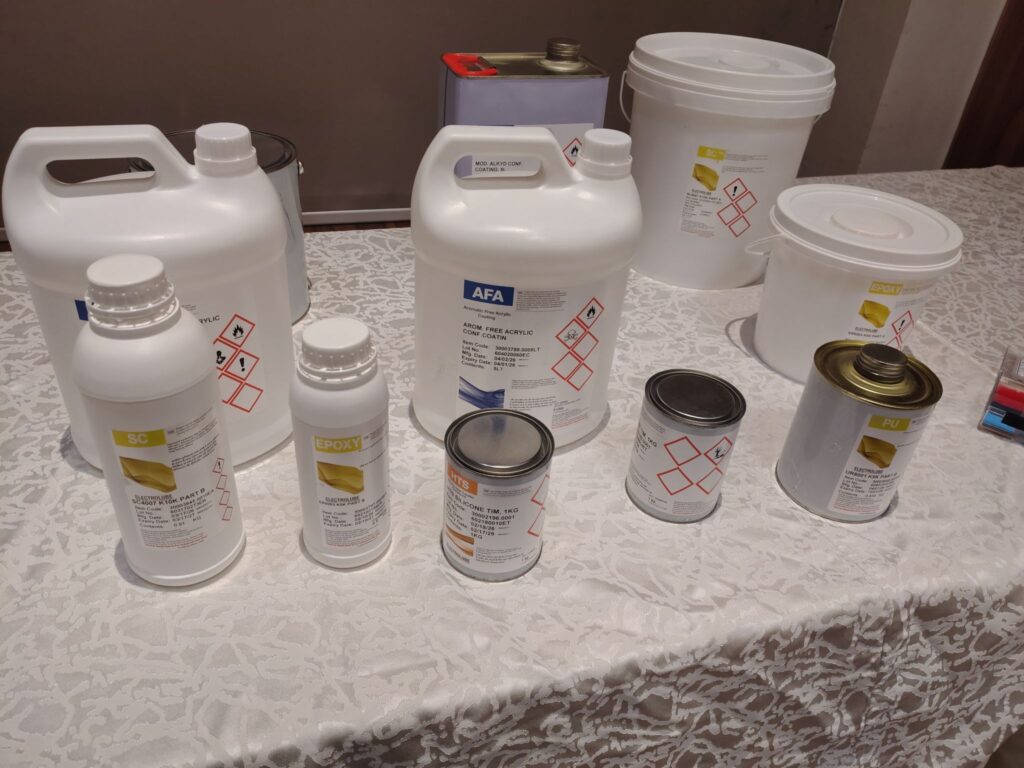
Conformal coatings, potting compounds, adhesives, sealants, and underfills each provide different forms of protection, making material selection dependent on the conditions an assembly will encounter.
“When we say selection of the right polymer for high reliability electronics, it is nothing but selecting the right polymer for the right application,” said Sharan Aiyappa, director, sales, MacDermid Alpha Electronics Solutions.
Electrochemical migration is one concern in densely populated assemblies. Moisture, residues, and electrical bias can contribute to conductive filament growth between closely spaced conductors, increasing the risk as component spacing decreases.
Aiyappa also highlighted cases where a coating had been applied but did not provide adequate temperature resistance for the operating environment. Under localised heat and water exposure, the material degraded, demonstrating why simply adding a protective layer is not sufficient. The chemistry, application process, and operating conditions all have to align.
Testing: Proving the Assembly Is Fit To Ship
The final stage brought the discussion from manufacturing inputs to the question of what leaves the factory.
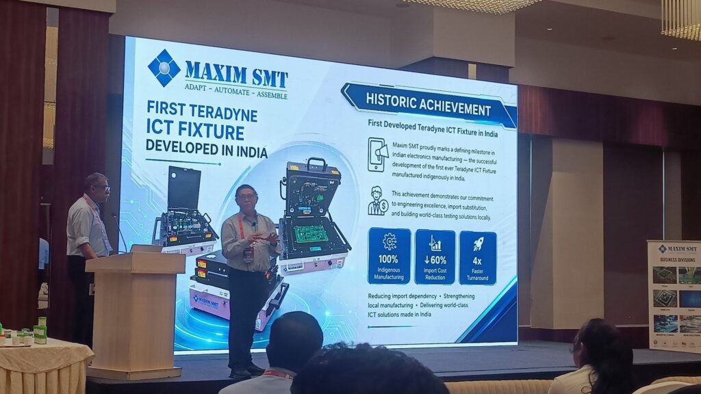
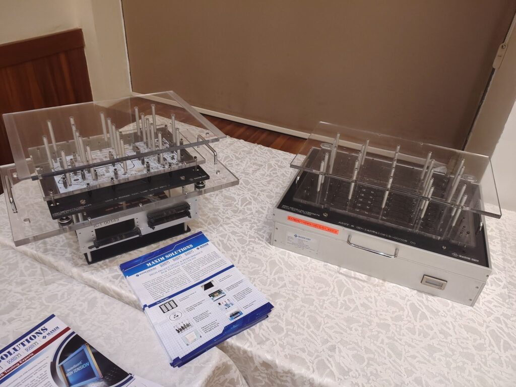
The final layer of process control is testing. Manufacturing defect analysis (MDA), in-circuit testing (ICT), functional testing, programming, vision inspection, calibration, and endurance testing can be combined depending on the product and the level of validation required.
MDA can identify opens, shorts, component presence, polarity, and passive-component values, while ICT can introduce powered measurements and extend into functions such as boundary scan, programming, and functional checks.
Yet testing becomes more challenging as assemblies shrink. Smaller boards can offer fewer accessible test points, while current requirements can complicate measurements. Test development can also depend heavily on the availability of complete schematics, layouts, board data, and other information from the manufacturer.
India’s testing ecosystem is still developing, according to C.H. Saw of Controlar.
“At the present moment, … India is at the learning age,” Saw said, pointing to the need for greater awareness of test systems and newer fixture methods. He also highlighted the continued use of manual data logging in some operations, where human intervention can introduce errors.
Saw expects India’s testing capabilities to expand, although cost remains a challenge because much of the required material is imported. “It’s a learning process,” he said, noting that cost will remain an important consideration as testing capabilities develop.
The larger manufacturing shift is therefore not about optimising one machine, material, or production stage in isolation. As electronics assemblies become more complex, manufacturers are increasingly required to control the complete chain: what material goes onto the board, how accurately it is deposited, how the assembly survives its operating environment, and how confidently its performance can be verified.
The opportunity lies in making each stage work more efficiently without creating a new weakness elsewhere in the process. That balance between cost, process control, and reliability is likely to remain central as electronics manufacturing moves towards increasingly dense and demanding assemblies.