Can an interface only atoms thick improve future transistors? Researchers have engineered the boundary between two materials to strengthen electrical control.
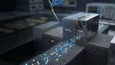
Researchers at National Yang Ming Chiao Tung University (NYCU) in Taiwan and TSMC Corporate Research have developed an ultrathin interface for transistors made from monolayer molybdenum disulfide (MoS₂). The approach uses a 0.42-nanometre aluminium oxide buffer layer between the atomically thin semiconductor and a high-κ hafnium oxide gate dielectric.
The work addresses a challenge in scaling two-dimensional transistors. As semiconductor channels become thinner, controlling charge through an equally thin gate dielectric becomes difficult because defects and unwanted interactions at the material interface can degrade electrical performance.
The engineered interface could improve electrostatic control while maintaining carrier transport in the MoS₂ channel. This is relevant to future transistor architectures that seek to move beyond the scaling limits of conventional silicon devices.
To build the interface, the researchers deposited an ultrathin epitaxial aluminium layer directly onto monolayer MoS₂ and then oxidised it to form the approximately 0.42-nanometre aluminium oxide layer. The researchers subsequently deposited high-κ hafnium oxide over the buffer layer. The aluminium oxide helps provide a more uniform surface for the dielectric while reducing unwanted electrical interactions at the semiconductor interface.
The team fabricated short-channel top-gate transistors using chemical-vapour-deposited monolayer MoS₂. The devices achieved an equivalent oxide thickness of about 1 nanometre and a maximum transconductance of 0.45 mS μm⁻¹, while showing low leakage current and minimal hysteresis. The reported channel length was about 100 nanometres.
The findings highlight the role of atomic interfaces in two-dimensional electronics, particularly as transistor dimensions shrink further. “Our research shows that the atomic interface between materials can be just as important,” says Professor Wen-Hao Chang, the study’s corresponding author from National Yang Ming Chiao Tung University.