




How do you get electricity into a semiconductor only a few atoms thick? A tin-based material can offer an injection route for both n-type and p-type devices.
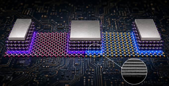
Researchers led by KAIST have developed a tin diselenide (SnSe₂) material that can efficiently inject charge into both n-type and p-type atomically thin semiconductors.
The material acts as a universal van der Waals tunnelling injector for monolayer tungsten diselenide (WSe₂) and molybdenum disulfide (MoS₂). This could simplify the electrical connections needed for smaller, stacked semiconductor devices.
The key advantage is that the same injector works with both types of transistor. Conventional approaches generally require different charge-injection conditions for n-type and p-type devices. SnSe₂ instead forms a weak van der Waals interface with the ultrathin semiconductor, helping reduce interface damage while allowing charge to enter efficiently.
The researchers demonstrated the approach using two materials. In p-type WSe₂, SnSe₂ enables interband tunnelling for charge injection. In n-type MoS₂, an electric field narrows the energy barrier, allowing electrons to tunnel through.
The improvement was significant. A p-type WSe₂ transistor using SnSe₂ achieved more than 1,000 times higher maximum drive current than a comparable device using nickel electrodes. An n-type MoS₂ transistor achieved an on/off current ratio exceeding one billion, providing strong control between conducting and non-conducting states.
The team also combined the two transistor types to build a CMOS inverter and demonstrated stable operation under repeated electrical signals. This shows that the material can support circuit-level operation, rather than only improving individual transistors.
The approach could help 2D semiconductors move towards higher-density and lower-power electronics, particularly as multiple ultrathin layers are explored for future AI and computing hardware. The researchers are now looking at direct-growth and large-area processing to support practical integration.
“This study demonstrates that the most challenging bottleneck for charge injection in monolayer 2D semiconductors can be addressed using a single material,” says Professor Seo Jun-gi of KAIST. “If direct growth and large-area processing technologies are combined in the future, it could accelerate the practical implementation of low-power 2D CMOS integrated circuits.”

