




Can stacked chips hide defects that conventional inspection misses? Inspection and wafer correction systems target two manufacturing challenges affecting advanced semiconductor packaging.
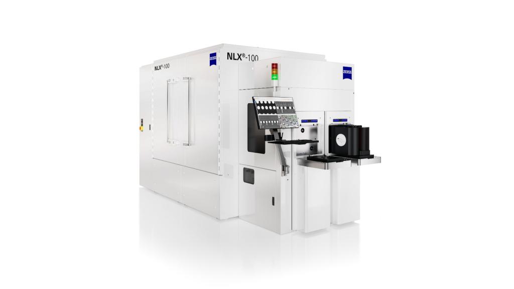
ZEISS SMT has introduced solutions for non-destructive X-ray inspection of internal chip-package connections and correction of wafer deformation, addressing process-control challenges in advanced semiconductor manufacturing.
As manufacturers integrate multiple dies or chiplets into compact packages, inspecting internal connections and controlling wafer shape become increasingly important for production yield. Defects in connections between stacked dies can compromise package reliability, while wafer deformation can complicate downstream processing and bonding. These challenges require inspection and correction technologies that help manufacturers identify problems before they affect subsequent manufacturing stages.
The ZEISS NLX system uses X-ray inspection to reveal internal structures in semiconductor packages without destroying them. It enables manufacturers to inspect connections between stacked dies and identify potential defects at an early stage. Designed for 300-millimetre wafers, the system supports both the development of new manufacturing processes and high-volume production. Its non-destructive inspection capability allows internal package structures to be examined without sacrificing the component being inspected.
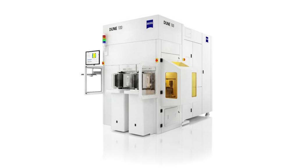
The ZEISS DUNE system addresses wafer bow, a deformation that can affect complex semiconductor manufacturing processes. It measures wafer topography and enables individual correction based on the wafer’s shape. This supports wafer preparation for bonding and can help prevent yield losses during downstream processing. By combining measurement with targeted correction, the system addresses wafer-shape variations that could otherwise complicate subsequent process steps.
The two systems form part of ZEISS SMT’s broader semiconductor manufacturing portfolio, which includes lithography optics, photomask inspection and repair solutions, and technologies for advanced packaging.
Christoph Hensche, President of ZEISS Semiconductor Manufacturing Optics and member of the ZEISS SMT management team, says, “The next generation of semiconductor manufacturing will not be enabled by individual technology leaps alone, but by the precise interaction of many highly complex process steps.”
Click here for the official announcement.