Setting units and grids. The taskbar contains eight shortcuts for various file and edit options along with five dropdown menus for setting units and grids used by FreePCB—units for selecting sizes in mils or mm for dimensional units, Visible to set the spacing of a rectangular array of dots in the layout window as a visual reference, Placement to set a snap grid for placing parts, text, etc, Routing for setting up a snap grid for routing traces and drawing copper areas and Angle to set a snap angle (in degrees) for routing and drawing poly-lines such as the board outline and copper areas.
Note: When a project is created, the default values for all are copied into the options section of the project file. They can be modified by editing either default file default.cfg in the folder which contains FreePCB.exe or the project file using a text editor.

Layer list. The top vertical list to the left of the layout area is the layer list. It contains all drawing layers that are in use by the project, with boxes next to each layer showing its colour and visibility. If the layer has been made invisible, the square will be white with an ‘X’ through it. Also, you can toggle each layer from visible to invisible by clicking on the square.
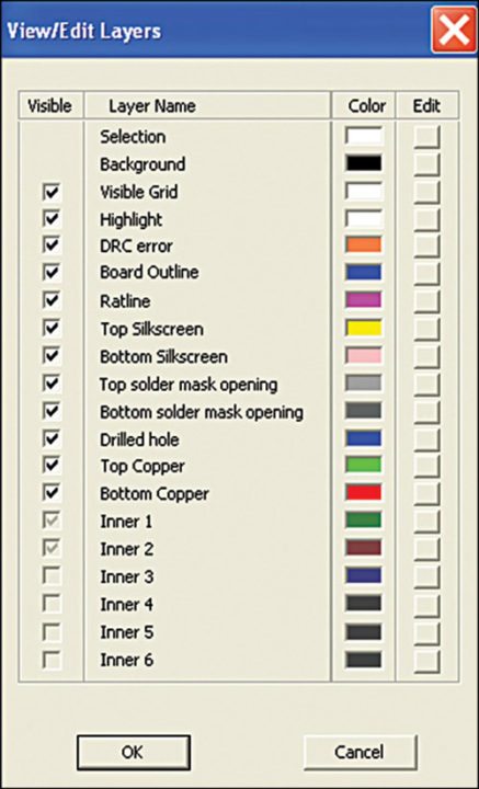
The active layer for routing can be identified as one with an arrowhead. You can change the active routing layer by pressing a numeric key on the keyboard, or by clicking on the name of the layer in the list.
Selection mask. The selection mask is below the layer list, with boxes to enable/disable selection of various items. For overlapping items, it may be difficult to make the required selection. here you can use the selection mask to enable or disable the selection of different item types. A green box means that the item type can be selected, while a red box means that it cannot. You can toggle the state of each box by clicking on it.

The netlist
A set of pins which are connected together by lines on the schematic is a net. Each pin in the net is identified by the reference designator of the part containing the pin, the character dot (.) and the pin name. For example, pin 8 on part U5 would be U5.8.
If the schematic was created with a schematic editor, the part list and netlist can be automatically written to a netlist file. Netlist files are available in various formats. You should choose a format which is recognised by FreePCB, such as PADS-PCB. If you are working from a printed or hand-drawn schematic, you will have to manually make the netlist file in a text editor.
Rubber-band lines. When you import the netlist file into FreePCB to start your design, FreePCB will try to find a footprint to match the package identifier for each part, or you can assign footprints manually, or go back and edit the netlist.
All of the footprints will be placed near the lower left corner of the PCB design area. After loading, connections will appear as rubber-band lines between the pins, called Ratlines. Moving parts will move these ratlines too, and make it easier to manage connections.
Adding parts and nets on-the-fly. Alternatively, you can create a design in FreePCB without a netlist file by using the on-the-fly editing technique. Starting with an empty design, you can add each part, net and connection using the Modify and Add menus. Reference designators and net names will be necessary. This is handy in designing small designs but for larger designs creating a netlist file should be preferred.
Placing parts. Parts can be placed on the PCB by moving or rotating them, as necessary, and the ratlines will automatically be reassigned to minimise their total length. Using a snap grid will make the alignment of parts easier.
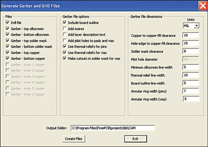
Finally, the plot and drill features
FreePCB allows plots of each layer to be exported as Gerber files, which are used to make photographs for PCB fabrication. FreePCB also produces drill files, which specify all the holes to be drilled in the board. You just need to select the files that you want to generate and click on Create Files, which will write the drill files to your output folder. There is also a Panelising section that allows you to select the number of copies to be produced in each direction and the spacing between copies.
Download latest version of the software: click here
The author is a technical journalist at EFY