


For any electronics product, printed circuit board (PCB) forms the basic foundation for interconnecting and packaging. PCBs are used to mechanically support and electrically connect electronic components using conductive pathways, tracks or signal traces etched from copper sheets laminated on a non-conductive substrate (source: Wikipedia). PCBs are also referred to as printed wiring boards (PWBs), or etched wiring boards, which have evolved over the years from uncomplicated single- and double-sided plated-through-hole (PTH) to become multi-layered PCBs.
The fortunes of the PCB industry depend on the health of IT, telecom, automobile, electronic gaming and consumer electronics. Due to the rapid growth of the electronics industry worldwide, the global PCB market has witnessed a remarkable growth over the last two decades.
What’s the market like?
Japan and Asia-Pacific collectively contribute a major share to the global PCB market. Amongst Asian countries, India and China are central to the growth of the PCB industry, thanks to the rapid expansion of electronic manufacturing bases. This growth is triggered by the shifting of production activities and facilities of key multinational players in these countries.

The demand from automotive electronics segment drives a positive outlook for the PCB market over the next few years. As electronic components account for a fair portion of the overall value of materials consumed in cars’ production, the stage seems to be well set for robust growth in the PCB market in near future. “Without PCB, we can not expect any electronic circuit. Since a PCB provides physical support as well as interconnections between different electronic components, there exist great opportunities as well as very good growth in this field worldwide,” says Shavinder Singla, deputy engineer in PCB Lab at Centre for Development of Advanced Computing (CDAC), Mohali.
K. Krithiga, technical lead at CADD Center, adds, “For electricals and electronics engineering (EEE) and electronics communication engineering (EC) students, this is a good field to start their career. What they have studied during their engineering course, they should apply to circuit design and PCB design. Initially, engineering graduates can enter into this field as a circuit designer or a board designer.”
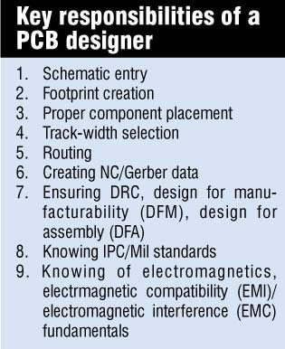
A glimpse
PCB designers are key persons in research and development (R&D), electronics production units as well as in the PCB industry. A PCB designer’s job comes with a lot of responsibilities. “Nowadays it’s not only about making interconnections between electronic components but also understanding the functioning of the circuit. It is often observed that a circuit which functions well when assembled over a bread board may or may not function properly over a poorly designed PCB layout. Depending upon the complexity of the circuit or PCB it may take two to three days for system engineers to locate and rectify the problems,” Singla says.
There can be numerous reasons for such kind of failures; PCB design and fabrication being one of them. “If a PCB is not designed or fabricated as per the circuit requirements, the circuit may not function at all, or function partially. Generally, circuit designers overlook the PCB design/fabrication part so as to reduce the product’s time-to-market or to compensate for the delay. Sometimes PCB designers or fabricators are not allowed to devote sufficient time as intended,” Singla explains.
[stextbox id=”info”]
“Without PCB, we can not expect any electronic circuit. Since a PCB provides physical support as well as interconnections  between different electronic components, there exist great opportunities as well as very good growth in this field worldwide.”
— Shavinder Singla, deputy engineer in PCB Lab at Centre for Development of Advanced Computing (CDAC), Mohali

“For electricals and electronics engineering (EEE) and electronics communication engineering (EC) students, this is a good field to start their career.”
— K. Krithiga, technical lead, CADD Center
[/stextbox]
According to Vikas Kohli, senior architect, Cadence Design Systems India, “New computing, network, and telecommunication products have ine-radicably altered the PCB design landscape. A recent report titled ‘Design Trends and EDA Tool Usage—Asia Pacific,’ highlights consumer electronics, telecom/data communications and industrial control/medical electronics as dominant industries in the region. The PCB design section report shows that over 50 per cent of designs have less than 50 integrated circuits (ICs) on a board. In fact, 20 per cent of designs have less than four ICs on the board. The pin-count of these devices has increased, so has the complexity of the logical interconnects. In this case, a smaller number of larger components means a larger number of design headaches.”
“One design discipline greatly affected by this change is schematic design capture. To keep pace with shrinking market windows in light of all this complexity, designers have to capture designs faster than ever before. And to meet profitability goals they have to design it right the first time,” Kohli adds.
What your pocket says
Let’s turn to money matters. This field offers enough provisions for learning as well as earning. The starting salary for a fresher is typically between Rs 150,000 and Rs 200,000 per annum with impressive year to year hikes. Coming to experienced professionals, the PCB industry offers salary in the range of Rs 500,000 to Rs 600,000 per annum for people with four to five years of experience.
“As a fresher one can not expect high salary. But after an experience of five-six years, and with understanding and implementation of standards, one can expect a very good package and may act as a team leader,” adds Singla. And of course if you grab an international opportunity, the pay is quite good even for freshers. It is needless to mention that PCB designers can experience much better growth while working with an MNC.
“It’s been my experience that the designers who work on the higher-end or more expensive CAD tools (i.e., Cadence Allegro and Mentor Graphics) seem to get paid a little higher than designers who work on the lower-end or less expensive systems like Altium and PADS. As I mentioned earlier, back in the late 90s, as long as you were a good designer you would be hired regardless of the CAD tool. But now, unfortunately, hiring-managers seem to put an emphasis on which CAD systems you’re running and even what version, etc,” opines Derek Doucette, an executive with American Contract Group, a Massachusetts-based staffing firm. He has been placing candidates into PCB design positions since the 1990s.
“A designer once told me, “Besides a few features here and there, they basically all do the same thing.
 You just need to find out where they place the buttons.” I believe that if you are a good designer on one CAD system, with a slight learning curve, you should be able to pick up another system with no problem,” Derek told PCBDesign007 in an interview.
Who’s hiring?
It is difficult to point out a particular industry as the major recruiter of PCB designers. Aspirants in this field may look for opportunities in all industries which are directly involved in manufacturing electronics products. These include telecom, automotive, biomedical equipment, computer hardware, electronic security systems, consumer electronic appliances, mobile companies, industrial automation and power electronics, amongst others.
“The big organisations always have a team of six-eight designers while the middle ones have two-five designers. The team size depends upon the development of new hardware or modification of the existing one, and also on the size of the R&D team. However, to name a few, some of the major recruiters in this field are Bharat Electronics Limited, Semiconductor Complex Laboratory, HCL, L&T, GE, HP, Beetel, Nokia, Samsung, LG, Ericsson, Sony and Philips,” informs Singla.
Krithiga adds, “Small-sector PCB design companies are recruiting freshers. MNCs like Wipro, Applied Materials, TCS, Ingersoll Rand, and most of the electronics goods designing companies offer a good opportunity for PCB design engineers.”
Getting the job signal
Recruiters look for electronic and information engineering (EIE), EEE and ECE engineers with basic electronics components knowledge with any board design software like OrCAD, Allegro, Altium or PADS. At present, most of the companies are using Or-CAD and Allegro for circuit board design.
A PCB designer’s ‘must haves’ as stated by Singla are as follows:
1. Understanding of the functioning of an electronic circuit.
2. Knowledge of IPC/Mil standards.
3. Know the process of PCB manufacturing, assembling and testing.
4. Good knowledge of various electronic components’ packaging.
5. Know about different PCB base materials.
6. Able to interact with circuit designers, PCB manufacturing and assembling team.
7. Knowledge of EMI/EMC.
If the PCBs are not designed properly, one runs the risk of facing a high level of rework/rejection of populated or unpopulated PCBs. “I have also seen a lot of circuit malfunctions/ failures in the field, which are a result of poor design, fabrication or soldering techniques,” Singla says. He also suggests that PCB designers should have a detailed knowledge of not only PCB fabrication but also soldering techniques. Also, they are required to be kept abreast of the limitations of PCB manufacturers with respect to minimum drill-size, minimum track-width, minimum track-to-track and track-to-pad distance, tolerances, etc.
Feel interested? Check out the career guidance section for more.


Helpful article. Thank you.
If possible, could you kindly suggest on well taught PCB design courses in Mumbai ?
Any help would be much appreciated.
Sorry, we cannot help you personally but we’d recommend you to join our forum (https://www.electronicsforu.com/forums) and post your question there. Our community members could help you out. Registering is just one-click and free through ‘FB Connect’. You could also post your question on our timeline.
Did u do PCB design course in Mumbai. Even I am looking for the same. Can u help me out ??
in mumbai at saitech systems
nice article
I am very interested to work in PCB design related job, I have learned OR-CAD during diploma, now I am completed btech in ECE, please can you suggest me how to get a job in this field. In Hyderabad and Bangalore
Pcb layout design job has a scope in future or not. I’m in confused with it.I have joined in startup company. My salary is very low. Shall i work it or shall i change my career path. Please reply me