


Reference Design For A Handheld TDS Metre that employs the direct measurement of the conductivity of the solution technique to detect TDS.
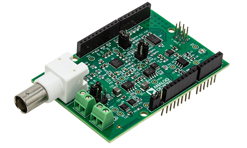 Consumption of contaminated water poses various health risks. One of the ways to find contaminants is by measuring the amount of total dissolved solids (TDS) in the water. Any particle greater than the size of 2 microns is considered TDS. CN0411 from Analog Devices is a reference design for a compact TDS measurement system. The TDS monitor uses the direct measurement of the conductivity of the solution technique to detect TDS. The main advantage of this design is that it uses a standard BNC probe connection making it both faster and cheaper to design.
The reference design utilises a 16-bit SPI voltage DAC and an ultra-low on-resistance CMOS Dual 2:1 SPDT switch to generate a bipolar square wave excitation across the conductivity probe. The frequency of the excitation is controlled by a PWM signal from the microcontroller which can be set to either 2.4 kHz or 94 Hz via the system software. The reference design is also Arduino form-factor compatible.

For higher accuracy, the reference design features temperature compensation that is performed using either a 100 Ω or 1000 Ω 2-wire RTD. The design is capable of measuring low to high conductivity levels ranging from 1 μS to 0.1 S and can accommodate 2-wire conductivity probes of different cell constants from 0.01 to 10.
This design uses a combination of components that allow for single supply operation which minimizes circuit complexity, making this suitable for low-power and portable instrument applications. Applications include chemical water analysis for field research, and monitoring water systems and natural bodies of water.
The capacitance and polarization effects of the electrodes in the conductivity cell require that the excitation signal be a bipolar square wave with a sufficiently high frequency to reduce polarization effects but also with sufficiently long periods to reduce capacitance effects. To avoid damaging the conductivity electrodes, the signal must have a very low to zero dc offset and magnitude. The system can measure low to high conductivity levels ranging from 1 μS to 0.1 S
This reference design has been tested by ADI. It comes with comprehensive software, firmware libraries, tools, battery, etc. You can find additional data about the reference design on the company’s website. To read more about this reference design click here.
