
As electronic systems become more complex and integrated into nearly all the devices and networks we interact with today, the importance of systems reliability — and the costs of systems failure — are greater than ever before. If a system fails, it can not only cost companies millions of dollars in repair and warranty costs, it can be fatal. Take, for example, the AirAsia flight that crashed in December 2014, killing all of its 162 passengers and crew. The official report concluded that the sequence of events leading to the crash began with a tiny crack, caused by thermal stress and fatigue, in a soldered electrical connection on a printed circuit board (PCB)1.
Thermal stress is a leading cause of PCB damage, so it is a constant concern in PCB design. It is caused by the difference in the coefficient of thermal expansion (CTE) for the copper and the epoxy resin typically used in a PCB. As the temperature changes from hot to cold in repeated cycles, the solder balls that provide contact between the PCB and the integrated circuit (IC) package are stretched and squeezed. This can cause separation from the IC package or the PCB, leading to disastrous electrical failure.
In the past, it was not practical to accurately simulate the amount of thermal deformation of a proposed board design and accurately identify areas affected by thermal stress. Engineers had a choice between two techniques, a low fidelity “lumped” and a high fidelity “explicit” approach.

With the “lumped” approach, you reduce the complexity of the model by building an approximation of the board’s individual components and giving all the layers of the PCB the same material properties. Since the multitude of traces and vias are not discretized the mesh count is much lower, solver time is reduced. However, the results are not very accurate and you probably won’t be able to pinpoint large heat gradients and areas of stress concentration.
WIth the “explicit” approach, you discretize the entire board with all the thousands of traces, vias, and other interfaces. While this approach may yield a highly accurate solutions, the time to prepare the mesh and compute the solution is often impractical, particularly in early design iterations.

The Efficient “Metal Trace Mapping” Technique
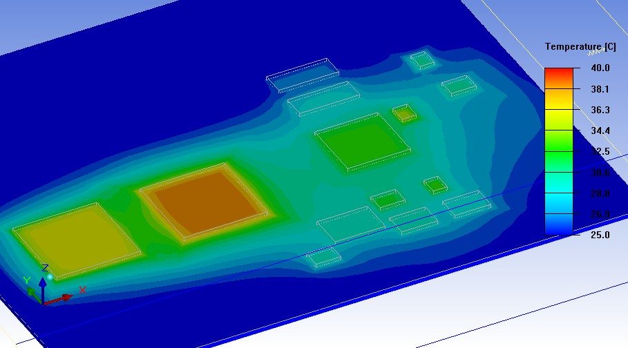
ANSYS has overcome the deficiencies of the previous two approaches with a new multiphysics methodology that simplifies PCB geometry while accurately representing its material properties at any point. This technique, called “Trace Metal Mapping”, efficiently simulates board performance under thermal loading. With this technique, a hexahedron mesh is initially created which discretizes each layer of the PCB, ignoring the interfaces between the thousands of metal traces and silicon. Next the ECAD information is imported and the material fractions for each element are calculated and mapped onto the mesh. The result is a fast, easily defined mesh and mapping that takes only minutes to set up. Using ANSYS Icepak, the temperature fields on and around the board are then determined using CFD (Computational Fluid Dynamics). You could then apply these temperature fields to the model as input conditions for a coupled thermal-stress analysis in ANSYS® Mechanical™. Just as importantly, you can create the model and run the analysis on a single simulation platform, which greatly simplifies the entire process.
Computing DC Solution
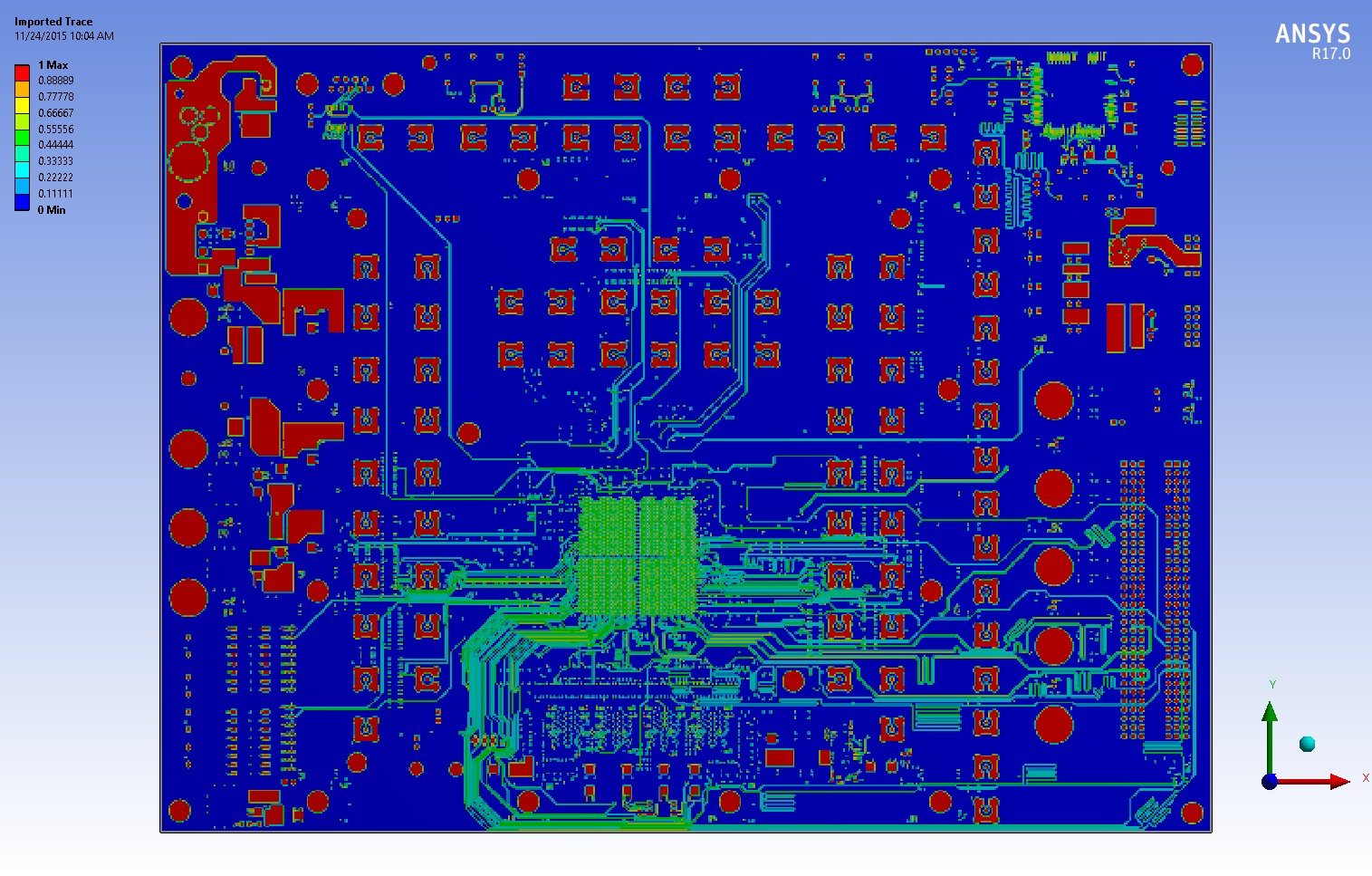
The first step is to use ANSYS SIwave to compute DC currents and voltages throughout the PCB. SIwave then calculates the current density throughout the board which in turn determines Joule heating (the process by which heat is produced due to electrical resistance when an electrical current flows through a conductor). Joule heating has increasingly become important as a source of thermal loading in PCBs as board sizes are reduced and power consumption remains steady or rises.
Performing Thermal Simulation New integration between SIwave and IcePak
With the release of ANSYS 17.0, the SIwave and Icepak bidirectional workflow has been integrated and automated, making it much easier to determine Joule heating. This capability imports the board, trace map and current density predictions, and sets the thermal boundary conditions for Icepak. Icepak uses the trace map to calculate the orthotropic thermal conductivity of the PCB. This is important because much of the heat generated on the board is dissipated via convection or radiation from the board itself and the material makeup of the board has a directional nature. Icepak solves fluid flow equations and includes all modes of heat transfer — conduction, convection and radiation — to compute temperatures at every point in the solution domain. The macro then exports the resulting temperatures from Icepak back into SIwave, which updates the electrical properties for the DC solution based on the temperature field. SIwave then recalculates the DC field and exports it to Icepak. This iterative process continues until the power dissipation and temperature results have converged.
Calculating Trace Metal Fraction
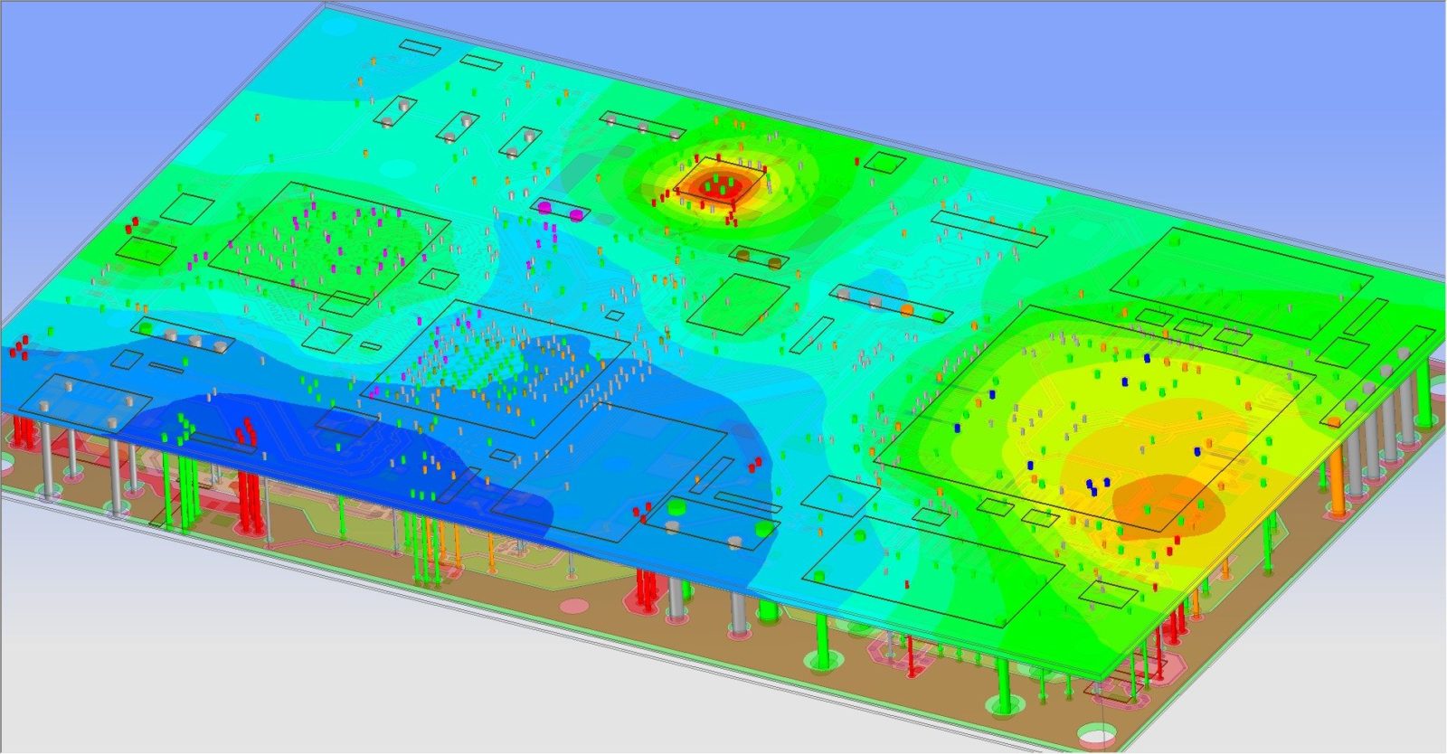
The next step is to build the structural model for computation of deformation, strain, and stress. ANSYS SpaceClaim reads the ECAD geometry converting it into a 3D model of simplified layers, mapping the metal and dielectric properties onto the layers. That geometry is then opened in Mechanical where it is easily meshed due to the layer nature of the geometry. Each layer can have a combination of metal and dielectric properties. Some elements will be entirely metal, others entirely dielectric, and still others a mixture of metal and dielectric. The resulting mesh is a simpler swept hexahedron mesh, so you need only to adjust density to suit your purposes. A higher mesh density will produce a more accurate representation of the model and take more computational time. A lower mesh density takes less computational time and will be less accurate.
For greater insight into the accuracy of the model, you can also create a color-coded, source point cloud that takes advantage of the data map but is independent of the mesh, and assesses if a point is metal, dielectric, or something in between, enabling you to better understand thermal effects.
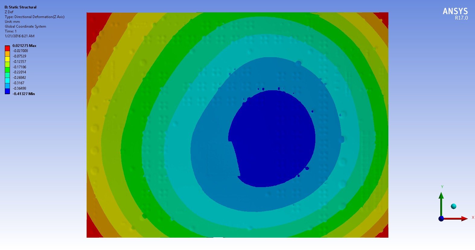
Calculating Thermal–Mechanical Stresses and Deformation
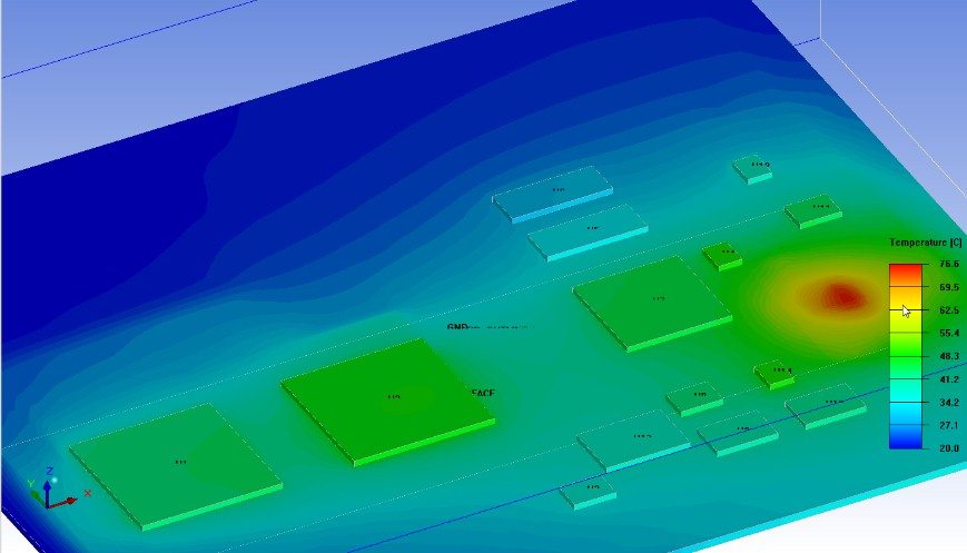
The resulting model with its mesh is the basis of a structural simulation with appropriate material properties taken into consideration. Its solution will quantify thermal stresses, strains, and deformation at any location on the board. By knowing these locations, you are able to determine whether some aspects of the model are at risk of failure, including attachment locations such as at solder balls. Icepak simulation also accounts for the cooling conditions of the board itself (for example, cooling fans). The engineer can also perform dynamic analysis to determine the modal frequencies and effects of random vibration on the board with thermal loading taken into account.
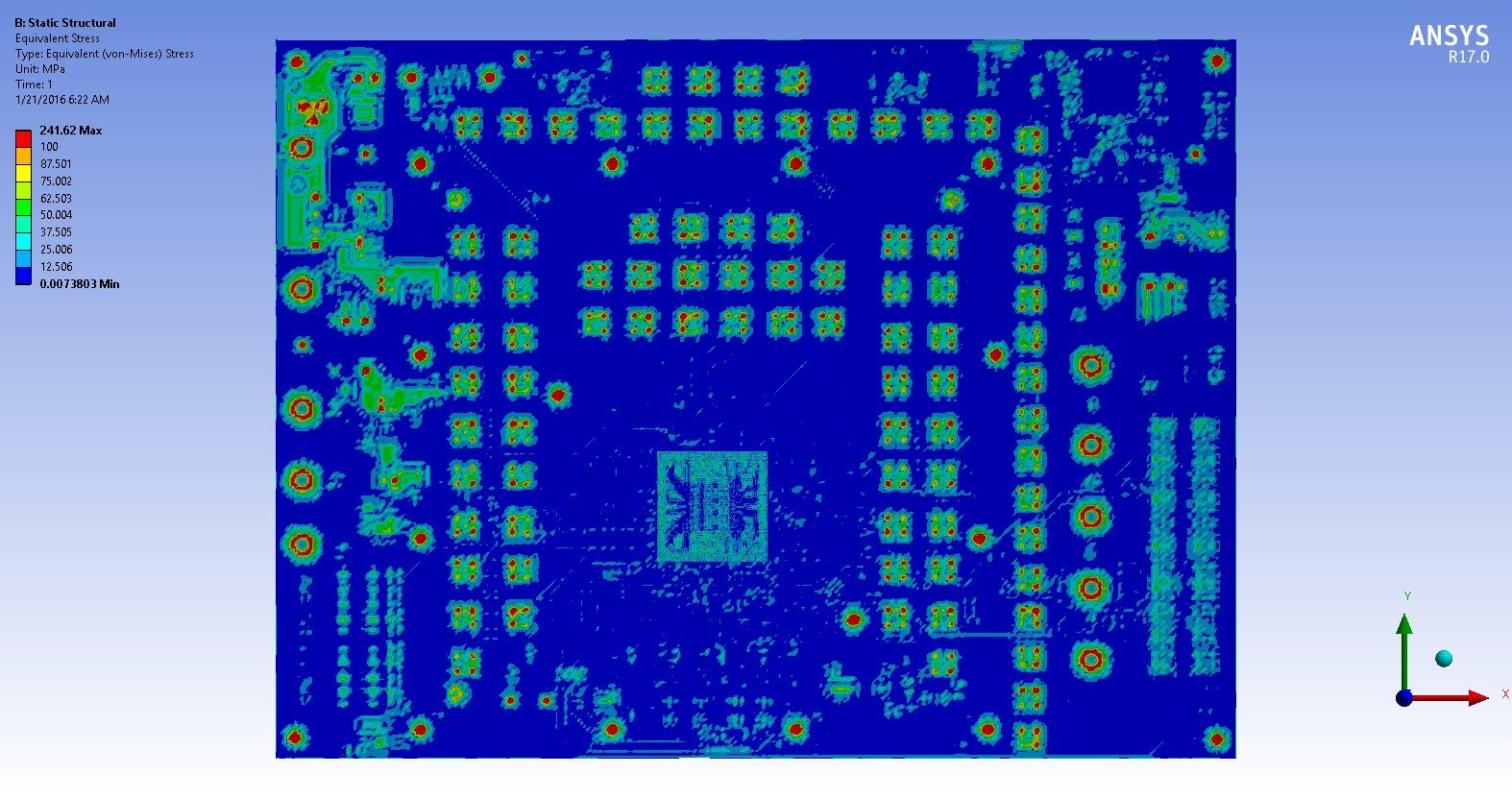
This multiphysics simulation methodology gives engineers the ability — for the first time — to accurately determine the effects of thermal loading on a PCB within a timeframe that is relevant to a typical design cycle. One sample model with 2194 parts (55 board, 35 package and 2104 solder balls) and 3 million nodes and 3 million elements took less than four hours to set up and 18 minutes and 37 seconds to solve. You can now identify thermal loading issues, propose possible solutions and determine whether or not each of their proposed solutions solves the problem long before a prototype is produced. By understanding the effects of thermal loading on the structural integrity and reliability of the board in the early stages of the design process, engineers are empowered to design products with lower failure rates and reduced warranty costs while also reducing time to market and engineering expenses.