


This article describes a low-cost low noise audio distribution  amplifier based on hybrid or mixed technology. Input to the amplifier is from low-noise, high-gain npn transistor. Output buffers are implemented with voltage followers using an operational amplifier (op-amp). The combination of low-noise transistor and push-pull output stage of the op-amp guarantees good characteristics of the hybrid amplifier.
Often we are required to send signals from one audio source to many loads/speakers. For that we use an audio distribution amplifier. This circuit employs low-noise bipolar transistor BC550 and op-amp LM324, which are widely available at low cost.
Audio distribution amplifier circuit
Buffers. The individual output buffers/followers of the op-amp work as push-pull output drivers separating the outputs from each other and the pre-amplifier from the loads.

Pre-amplifier: Common low noise pre-amplifier using BC550 guarantees low noise in the entire circuit. Common negative AC and DC feedback for the pre-amplifier and the first output buffer guarantee low total harmonic distortion.
Gain: Gain in the pre-amplifier can be set from one to more than 50 depending on the gain of the transistor and the resistors around it.

Common feedback of the pre-amplifier and the output buffer reduces the distortions of LM324.
The methods mentioned above are effective especially when all outputs of the amplifiers are of the same type and are loaded with the same or similar loads.
Circuit operation
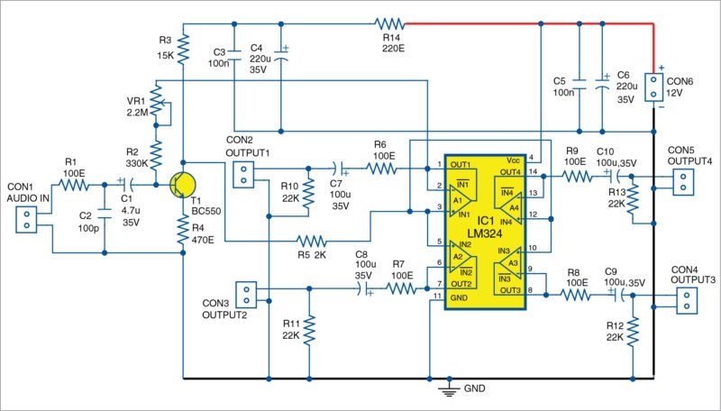
Fig. 1 shows the circuit of the low-noise audio distribution amplifier with four output buffers. Op-amps should be of the same type and preferably in  the same package. Resistor R1 and capacitor C2 are used to reduce RFI and EMI. Input amplifier stage is built around transistor T1 (BC550).
R14, C3 and C4 form filter circuit of the power supply for T1. Main feature of the circuit is the feedback implemented with R2 (330-kilo-ohm) and potmeter VR1 (2.2-mega-ohm) between output of the first buffer (A1) and base of T1.
R2 and VR1 implement AC and DC negative feedback, which set the initial working point of T1 and reduce distortions in the output stages. Collector current of T1 is usually selected in the range 0.2mA to 1mA, depending on the power supply.
Voltage gain of the amplifier is set to around 30 and can be calculated with the approximate formula given below:
Av = – R3/R4
Noise of the circuit depends practically only on the noise from the preamplifier stage around low-noise T1. Consequently, you would have low noise for the circuit. Alternatively, you can use noisy, low-cost but high-output-current op-amps as output buffers.
Power supply: Circuit is operational in full operation range of the op-amp and transistor. For LM324, operating range is from 3V to 32V. Power supply above 9V is preferable. Quiescent current of the circuit is low and is equal to the emitter current of T1 plus quiescent current of the op-amp. 12V DC power supply was used during testing.
Construction and testing
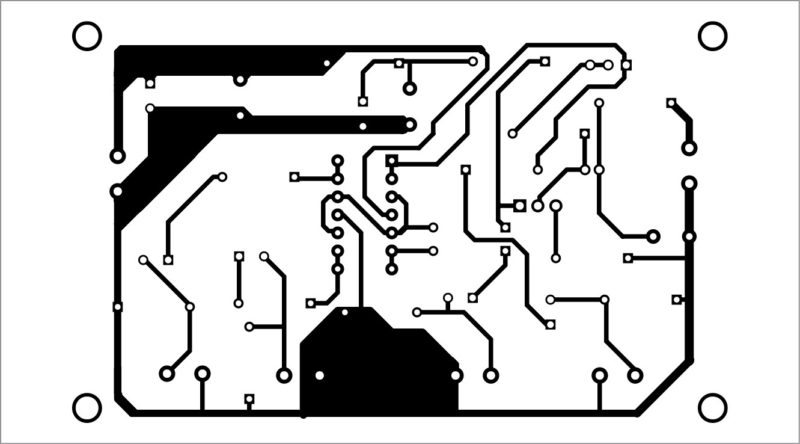
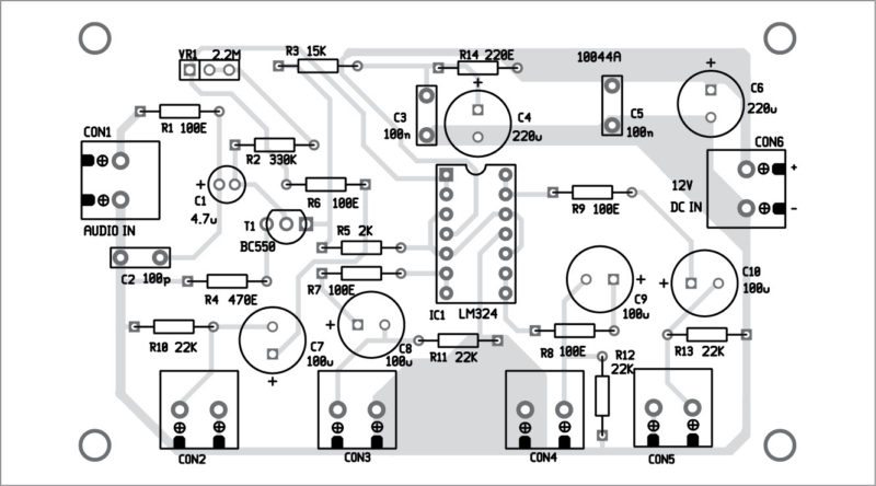
A single-side PCB pattern of the low-noise, low-cost audio distribution amplifier is shown in Fig. 2 and its component layout in Fig. 3.
For testing, apply well-regulated 12V power supply. First, short the input at CON1 (with no input signal) and vary VR1 till you get around half the power supply (6V) at collector of T1. Then, open the shorting input and apply a sine-wave signal around 1kHz with 10mVpp amplitude at CON1.
You can obtain a sine-wave with peak-to-peak amplitude depending on the selected gain at output pins 1, 7, 8 and 14 of A1, A2, A3 and A4 op-amps, respectively. You should get around 300 mVpp in all output pins.
Vout =(-R3/R4)×Vin
=30×10mVpp=300mVpp
You can replace VR1 and R2 with a single resistor of around 510-kilo-ohm if the power supply is 15V and transistor T1 is BC550C.
Download PCB Component PDF: Click here
Feel interested? check out other electronics projects.

can you please tell me what is the difference between Simple Audio Amplifier and Audio-Distribution Amplifier?
which types of audio devices should be used in con1,2,3,4,5,6?
Audio source like MP3 player or mobile phone can be connected at CON1. You can connect loudspeakers or audio power amplifier(s) at CON2 to CON6.
can you explain how to test input and out
What’s difference between this circuit & the headphone buffer circuit project by same author? Can both the circuits be used to connect multiple headphones?