
A ready-to-use RF power amplifier reference design delivers up to 100 W across 1.8 MHz to 250 MHz, featuring a reusable PCB layout, optimized thermal management, and comprehensive documentation for industrial, medical, and communication systems.
This reference design has been developed by NXP Semiconductors to provide engineers with a ready-to-use foundation for high-performance RF power amplifier systems. Its primary goal is to reduce development time, simplify prototyping, and ensure consistent results across a wide range of radio-frequency applications. By offering a validated and tested architecture, the design enables engineers to focus on system integration and optimization rather than starting from scratch.
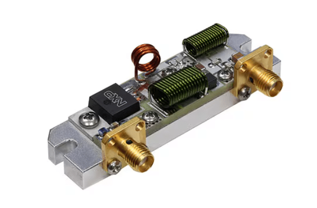
NXP has introduced the MRF101AN Reference Circuits, which support continuous operation across a frequency range of 1.8 MHz to 250 MHz, delivering output power of up to 100 W CW. This design emphasizes flexibility, efficiency, and ease of adaptation for multiple frequency bands. A major advantage is the reusable PCB layout, which allows engineers to modify a single design slightly to suit different operating frequencies, saving both time and resources. The architecture is optimized for balanced thermal performance, high linearity, and improved impedance matching, making it suitable for a wide range of industrial, medical, and communication applications. The reference design package also provides a complete implementation roadmap, including circuit details, tuning recommendations, and measurement data, which helps developers transition quickly from prototype to production.

The reference design includes several key features that make it practical for real-world applications. It offers wide frequency coverage from 1.8 MHz to 250 MHz, high continuous-wave output power up to 100 W, and supports PCB layout reuse for multiple frequency bands. Additionally, it comes with full documentation, including circuit overviews, tuning guides, test data, mechanical drawings, and performance graphs. These features allow engineers to integrate the design efficiently while maintaining high reliability and consistent performance. Typical applications include industrial, scientific, and medical (ISM) systems such as plasma generation, industrial heating, and medical RF ablation. It can also be used in HF and VHF communication systems, including transmitters and base stations, as well as RF-based power systems and switch-mode amplifiers where stable high-frequency operation is essential.
The architecture of the design follows a straightforward RF signal chain: RF input passes through an input matching network, enters the amplifier section, and then passes through an output matching network to drive the load. Each stage is optimized to maximize power transfer, minimize signal reflection, and provide effective thermal management. Input and output matching networks ensure stable operation and maintain system efficiency across the frequency range.
Along with the reference design, NXP provides a comprehensive set of resources, including schematic diagrams, PCB layout files, a bill of materials, measurement reports, tuning notes, and board photographs. These materials allow engineers to replicate and customize the design according to their specific system requirements. The complete design package and related documentation can be accessed here.