NFC (near field communication) is a short-range wireless technology that enables data exchange between two devices placed within 4cm of each other. In an NFC business card, a built-in NFC chip lets users instantly access contact details or a website by simply tapping the card with an NFC-enabled smartphone.
This system presents a universal NFC smart card based on the ST25DV64K-IER6T3 dynamic NFC/RFID tag IC. The versatile IC enables the card to function as a professional business card, employee ID badge, NFC memory storage device, or secure access token. However, it is not intended for certified banking or ATM applications because of regulatory and certification requirements.
The ST25DV64K-IER6T3 features 64-kbit (8kB) user EEPROM memory, which can be divided into up to four flexible, password-protected areas. It supports dual interfaces—ISO 15693/NFC Forum Type 5 for smartphone compatibility and a high-speed I²C interface operating at up to 1MHz. The IC also incorporates fast transfer mode (FTM) with a 256-byte mailbox for efficient data exchange between the RF and I²C interfaces, along with extensive configuration options for a wide range of NFC applications.
Although the primary objective of this system is to create an NFC business card for convenient sharing of vCard and NDEF messages, the card also supports energy harvesting through the V_EH pin. This feature can deliver approximately 2mW-3mW of power under typical conditions and up to 10mW-20mW under optimal conditions, making it suitable for powering low-current devices such as LED indicators without an external power source.
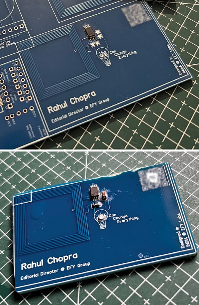
Features such as a programmable GPO interrupt, multiple 64-bit password-protected memory areas, 1 million write cycles, and 40-year data retention make the ST25DV64K-IER6T3 a reliable and future-proof platform for developing smart, interactive NFC cards. The prototype of the NFC smart card is shown in Fig. 1. The components required to build the system are listed in the Bill of Materials (Table 1).

Also check: DIY NFC smart ID card that needs no battery.
POC Video Tutorial
| Table 1: Bill of Materials | |||||
| Component | Desi-gnator | Footprint | Quantity | Manufacturer Part Number | Manufacturer |
| 10µF capacitor | C1 | 0805 | 1 | CL10A106KP8NNNC | Samsung |
| 2.7kΩ resistor | R1 | 0805 | 1 | 0805W8F2701T5E | Uni-Royal |
| NFC dynamic tag IC | U1 | TSSOP-8 (4.4mm×3.0mm, 0.65mm pitch) | 1 | ST25DV64K-IER6T3 | STMicroelectronics |
| Red LED | U2 | LED0603 | 1 | KP-1608SURCK | Kingbright |
| NFC antenna | U3 | PCB spiral antenna | 1 | Integrated on PCB | — |
NFC Business Card Circuit Design and Working
For an NFC business card, two key aspects require careful consideration: energy harvesting and antenna design.
Antenna design is critical in any NFC-based application. Best practices, design guidelines, and design tools are beyond the scope of this article and will be covered separately. Additional guidance can also be found in online technical resources. The discussion here focuses on selecting an appropriate NFC IC and the corresponding circuit design.
The ST25DV64K-IER6T3 dynamic NFC/RFID tag IC was selected for this system. Although several alternatives are available from NXP, including the NTAG and ICODE series, any NFC IC that provides a suitable balance of memory capacity, dual-interface communication (RF and I²C), and energy harvesting capability can be used. The ST25DV64K-IER6T3 offers an excellent combination of these features, making it well suited to this system.
According to the ST25DV64K datasheet published by STMicroelectronics, the IC provides 64-kbit (8kB) of user EEPROM memory, which can be divided into up to four password-protected areas. It supports ISO/IEC 15693 and NFC Forum Type 5 standards, ensuring compatibility with most NFC-enabled smartphones.
The IC also features an I²C interface supporting data rates of up to 1MHz, a 256-byte FTM mailbox for bidirectional communication between the RF and I²C interfaces, and an energy harvesting output (V_EH) for powering low-power external circuits. The ST25DV64K family is available in multiple package options. The compact TSSOP-8 package was selected for this system because it is well suited to both hand soldering and small-batch SMD assembly.
Fig. 2 shows the circuit diagram of the NFC business card. The design is based on the ST25DV64K-IER6T3 (U1) dynamic NFC/RFID tag IC, which is connected to the NFC antenna (U3) through the AC0 and AC1 pins. The antenna forms a resonant circuit that receives the 13.56MHz RF signal emitted by an NFC-enabled smartphone when it is brought close to the card.