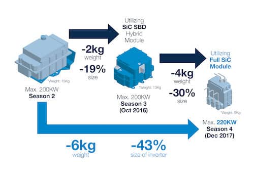
Semiconductor devices that exhibit wide bandgap characteristics, such as silicon carbide (SiC) and gallium nitride (GaN), are far more freely available and are becoming popular in high voltage, high power applications – such as the traction motors and inverters found in the automotive sector.
These devices allow higher voltages to be used (600V to 1700V) as well as the ability to operate at higher switching rates, both of which improve efficiency and reduce size and weight (which also improves vehicle efficiency). Efficiency is hugely important, especially in electric vehicles (EV) and hybrid electric vehicles (HEV) as it extends range and provides designers with options, such as the ability to use smaller battery packs in more compact vehicles.
However, using the new wide bandgap devices has required new standard CMOS drivers, which has necessitated a re-design of some elements of the power system. An additional challenge has been the need for new packaging types which has presented some difficulties with automotive qualification.
Benefits of SiC include a higher critical electric field, improved thermal conductivity and better dielectric constant – these are detailed in Table 1. As a result of these parametric enhancements, SiC devices have low on-resistance, reduced leakage current at all temperature levels, and generally perform better than silicon devices at elevated temperatures. Operation at faster switching speeds is possible with GaN devices, delivering higher efficiency due to their reduced electron saturation velocity.
![Table 1: Silicon vs silicon carbide and gallium nitride in power applications. [Source STMicroelectronics]](https://www.electronicsforu.com/wp-contents/uploads/2018/07/MRXA015Table1-500x354.jpg)
Transitioning to SiC
Compared to silicon, the 3eV bandgap of SiC has a breakdown field that is five times stronger and its thermal conductivity is over three times higher. The excellent performance / properties was the major reason that SiC became the first wide bandgap material to make its way into cars and trucks.
SiC devices have well-controlled switching times that do not vary appreciably with changes in temperature. As a result, less design margin is required to allow for temperature variation, allowing designers to achieve better performance from these devices. The ability to push the devices closer to their limit makes them ideally suited to applications such as the main inverters in EV and HEV.
Reliability is key in all automotive applications and, for that reason, diodes and MOSFETs are often qualified to AEC-Q101 to demonstrate their suitability. One such device is ROHM Semiconductor’s SCS220KGHR 1200V epitaxial planar Schottky diode. The device is available in TO-220 packaging and has a total capacitance (Qc) of just 65nC, allowing for high-speed operation with significantly reduced switching losses. Devices with lower voltage ratings, such as the 650V SCS215, can reduce system size due to the TO-263AB (also referred to as SOT-23) packaging.

Ford’s latest electric vehicle will be using 900V-rated SiC MOSFET devices from the Cree C3M0120090D series in a high power density, low-cost, on-board inverter. The motor systems in this vehicle are 88kW and the target running cost is said to be $8/kW for when mass production of the vehicle starts around 2020. In part, costs are being managed by reducing the overall weight, aiming to deliver 1.4kW/kg.
SiC devices were selected to deliver the very best on-resistance across the entire operating temperature range, as well as for their improved avalanche energy handling that is expected to increase reliability by a factor of 10x. The Cree MOSFETs have 10mΩ on-resistance and delivers better light-load efficiency than silicon IGBTs at low operating frequencies. As a result, the inverter losses are predicted to be 67% lower than an equivalent silicon solution. This dramatic reduction allows for vastly reduced cooling that will significantly reduce the size and weight of the inverter as well as the cooling costs.
GaN gains traction
GaN devices can achieve efficiencies as high as 97%, due in part to their higher bandgap (3.4eV) and higher electron mobility than SiC devices. Initially, GaN was adopted in RF applications due to their ability to perform well at elevated frequencies. More recently, GaN is now making inroads to power applications – especially automotive power.
Comparing GaN devices with silicon shows that they have comparable conduction losses per unit area to superjunction MOSFETs, but their switching characteristics are superior. Automotive-qualified GaN devices are now in production using enhancement mode device structures, giving these devices the ability to achieve efficiencies as high as 98%.One example of this technology is the GS6650x 650V GaN transistors from GaN Systems. These devices use enhancement mode GaN-on-silicon with a patented cell layout that enhances both the high current die performance and the yield. As a result, they support higher currents than SiC or silicon and allow for switching frequencies in excess of 100MHz. As well as their excellent electrical performance, they also have some novel thermal design features. Bottom-side cooling with low junction-to-case allows excess to be removed easily, especially in high power automotive inverter applications. GaNPX is a proprietary packaging technology that was developed to have a small 5.0mm x 6.6mm footprint with lower parasitic inductance and reduced thermal resistance than conventional packages. ROHM and GaN Systems are now collaborating on using the technology in next generation devices, demonstrating how important advanced packaging is in this area.
Qromis is a US-based start-up company that is using its QST substrate technology in the design of GaN power reference designs. This allows them to deposit thick, bulk-like GaN epitaxial layers onto 200mm wafers. The low defect rate that is achieved overcomes a major obstacle to performance and scalability. However, there are some challenges in migrating this to the automotive arena.
As EV and HEV need voltage ratings above 650V the buffer thickness required is greater. However, as the GaN and AlGaN epitaxial layers have differing coefficients of thermal expansion (CTE), there are challenges in achieving the higher breakdown voltage as well as the lower leakage levels. One approach to overcome this and achieve 900-1200V breakdown voltages would be to use thicker silicon substrates to avoid wafer warp. While this is possible, there are likely to be compatibility issues with some wafer handling equipment.

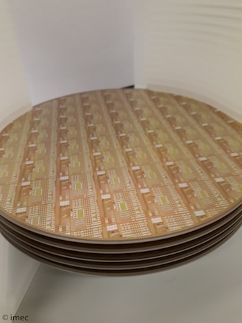
Once the thicker substrate challenge is addressed, then the device architectures required for lateral and vertical devices including rectifiers and monolithic and HV ICs will be possible. In pursuit of this goal, Qromis have collaborated with the IMEC microelectronics research institute in Belgium to build enhancement mode p-GaN power devices on their silicon pilot line. IMEC ported its p-GaN enhancement mode power device technology to the 200mm GaN-on-QST substrates in their silicon pilot line and demonstrated high performance power devices with threshold voltage of 2.8V.
As the thermal expansion of the QST substrates is very close to that of the GaN/AlGan layers, it has been possible to use standard thickness 200mm wafers to fabricate 900V to 1200V buffer devices. It is possible to deposit epitaxial layers that are more than 100 microns thick on the QST substrate, thereby enabling vertical GaN power switches / rectifiers that could be used in high voltage and high current applications. This approach would yield devices that would compete with silicon IGBTs, SiC power FETs and diodes on cost, removing a significant barrier to widespread adoption. As they use the AIX G5+ C system from Aixtron, the QST substrates from Qromis are fab compatible, eliminating handling problems.
The substrate can have epitaxial layers that are over 100 microns thick that would allow for vertical GaN power switches and rectifiers suitable for high voltage and high current applications where lateral GaN devices are utilised, competing with silicon IGBTs and SiC power FETs and diodes on cost. Qromis’ QST substrates are built using the AIX G5+ C system from Aixtron, resulting in fab-compatible standard thickness substrates for power devices.
GaN, AlN and LEDs
However, wide bandgap materials have more automotive applications than just power. For example, due to having a bandgap of over 6eV, aluminium nitride (AlN) is being used in alloy form alongside GaN LED devices. The combined technology is suitable for headlights and other lighting, such as cabin lighting, and has enabled 250nm ultraviolet LED emitters. Boron nitride (BN) is another wide bandgap material that is finding applications in substrates for high power electronics. It is additionally being used for fill plastics as it allows them to have reduced thermal expansion and higher thermal conductivity and well as electrical resistance.
Summary
Automotive-qualified wide bandgap SiC diodes and MOSFETs are now becoming mainstream and are to be found on vehicles that are in full production, where they contribute significantly to reduced power losses and increased operational efficiency. The technology is evolving and enhancement mode GaN MOSFETs offer very high switching rates and increase efficiency even further – up to 98%.
As substrate materials and manufacturing processes evolve then more device types will be possible including vertical and lateral designs. However, before this reaches the mainstream then certain packaging challenges and qualification issues will have to be fully addressed.


