
As demand grows for faster and more power-efficient chip connectivity, a newly taped-out USB IP aims to support next-generation AI, HPC, and mobile applications.
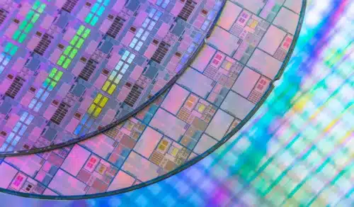
Taiwanese semiconductor IP provider M31 Technology has announced the successful tapeout of its eUSB2V2 interface IP on TSMC’s N2P process technology, marking a significant advancement in the development of next-generation semiconductor solutions.

The eUSB2V2 interface IP was developed in collaboration with TSMC and is designed to deliver high-speed connectivity while maintaining low power consumption. The solution remains compatible with the USB 2.0 ecosystem and supports operating voltages of 1.2V and 0.9V, making it suitable for advanced chip designs targeting artificial intelligence (AI), high-performance computing (HPC), and mobile devices.
According to M31, the interface incorporates programmable transmit de-emphasis and receiver equalization capabilities, enabling improved signal integrity and reliable performance at advanced process nodes. The technology supports data transfer rates ranging from 40Mbps to 4.8Gbps and has a target power consumption of 50mW under standard operating conditions.
The tapeout was achieved through co-optimization across design, circuit implementation, and physical layout, leveraging TSMC’s advanced-node development methodologies and reference flows. M31 said the collaboration helps streamline the path from design execution to production readiness while addressing the growing demand for efficient interface technologies in advanced semiconductor applications.
Scott Chang, CEO of M31, stated that the milestone reflects the company’s platform-driven approach to IP development and strengthens its ability to support customers building products on leading-edge process technologies.
As semiconductor manufacturers continue to develop increasingly complex chips for AI, HPC, and mobile workloads, demand is rising for power-efficient interface IP that can support higher performance requirements. M31’s latest tapeout contributes to the expanding ecosystem of advanced-node semiconductor technologies and reinforces industry efforts to accelerate innovation at the 2nm generation and beyond.